Water-level charged device model for electrostatic discharge test methods, and apparatus using same

a technology of electrostatic discharge and charge device, which is applied in the direction of individual semiconductor device testing, corona discharge, instruments, etc., can solve problems such as device failur

Active Publication Date: 2010-07-01
INTEL CORP
View PDF5 Cites 6 Cited by
  • Summary
  • Abstract
  • Description
  • Claims
  • Application Information

AI Technical Summary

Problems solved by technology

Charged device model (CDM) electrostatic discharge (ESD) events happen during the mechanical handling of integrated circuits and have often caused device failure.

Method used


Image

  • Water-level charged device model for electrostatic discharge test methods, and apparatus using same
  • Water-level charged device model for electrostatic discharge test methods, and apparatus using same
  • Water-level charged device model for electrostatic discharge test methods, and apparatus using same

Examples


examples

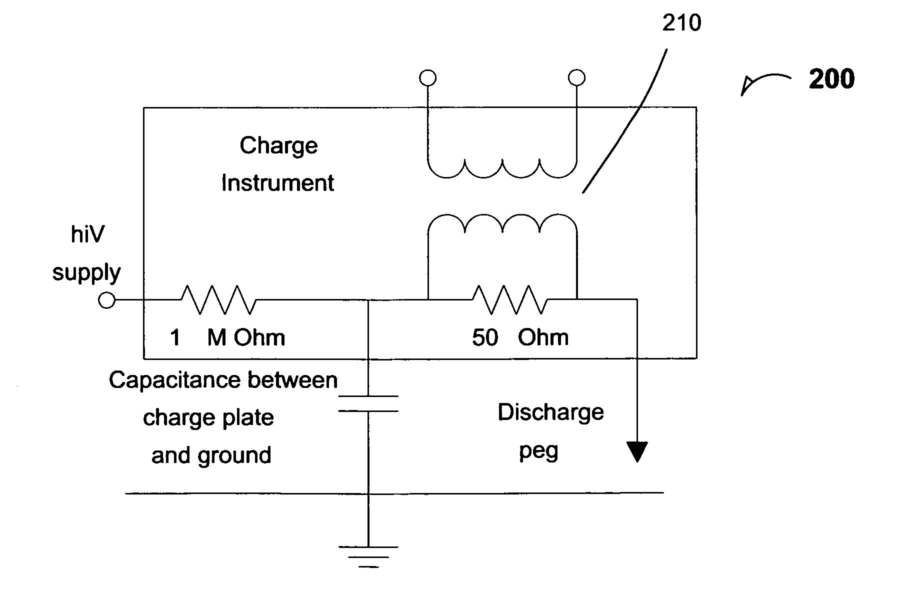
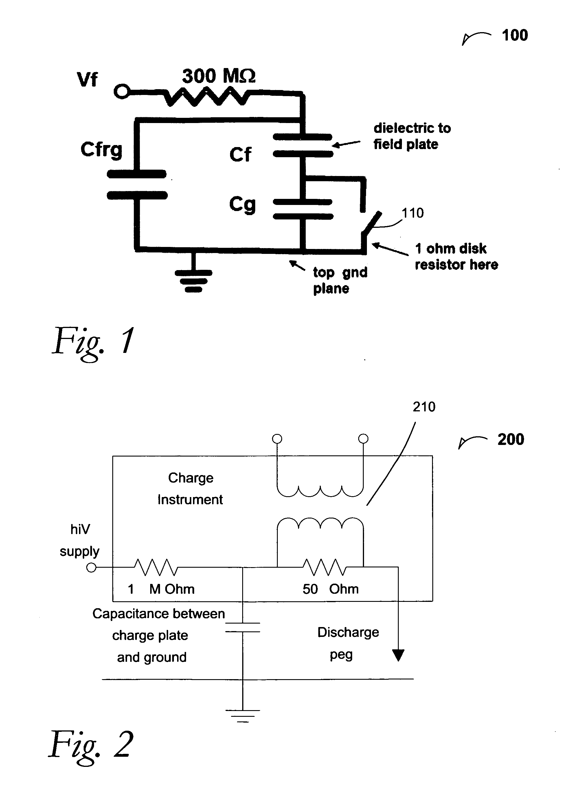
[0061]A known CDM defect existed on a pair of test pattern pins in Intel's 45 nm process. These were tested using a ns-CDM tester on a packaged device, with the low failure voltages shown in Table 1. WCDM testing was done for both positive and negative test voltages for both of the pins, using the smaller WCDM board (FIG. 5). CDM failure voltage is compared with the corresponding WCDM charge packet in Table 1. Voltage polarity for WCDM is reversed, to agree with current direction for the equivalent ns-CDM event.

[0062]Table 1 shows a consistently lower failure charge for WCDM testing, and for both methods usually a lower failure level for negative voltage. We have adjusted WCDM data for the extra 2 pF of transformer capacitance not seen by the scope. The failure voltages are in the same range for both pins and polarities; if anything, WCDM appears to have such a sharp rise time and high peak current that passing several nC should assure excellent CDM performance in a package.

TABLE IW...


PUM


Abstract

A charged device model (CDM) electrostatic discharge (ESD) testing is carried out at wafer level. Wafer CDM pulses are repeatedly applied and monitored. The wafer CDM (WCDM) pulses are accomplished with a probe-mounted printed-circuit board and a high-frequency transformer that captures fast CDM pulses. Modeling of CDM and WCDM in the time and frequency domain illustrates the dominant effects, and shows that WCDM can reproduce all the major phenomena of package-level CDM testing.

Description

TECHNICAL FIELD[0001]Disclosed embodiments relate to charged device model electrostatic discharge event apparatus and methods of using them.BACKGROUND[0002]Charged device model (CDM) electrostatic discharge (ESD) events happen during the mechanical handling of integrated circuits and have often caused device failure. CDM testers have been developed to test the effectiveness of the ESD protection circuitry. CDM testers have also relied upon radio frequency emission evaluation CDM ESD events.BRIEF DESCRIPTION OF THE DRAWINGS[0003]In order to understand the manner in which embodiments are obtained, a more particular description of various embodiments briefly described above will be rendered by reference to the appended drawings. These drawings depict embodiments that are not necessarily drawn to scale and are not to be considered to be limiting in scope. Some embodiments will be described and explained with additional specificity and detail through the use of the accompanying drawings ...

Claims


Application Information

Patent Timeline
Patent Type & Authority Applications(United States)
IPC IPC(8): H05F3/00
CPCG01R31/001
Inventor MALONEY, TIMOTHY J.CHOU, BRUCE C.
Owner INTEL CORP
Why Eureka
Try Eureka