Method for forming fine pattern using quadruple patterning in semiconductor device

a semiconductor device and quadruple patterning technology, applied in the field of semiconductor device fabrication, can solve the problems of limiting the resolution of photo-exposure equipment, the difficulty of current photo-exposure equipment to form fine patterns, and the limitation of the micronization of patterns

Active Publication Date: 2010-07-01
SK HYNIX INC
View PDF6 Cites 34 Cited by
  • Summary
  • Abstract
  • Description
  • Claims
  • Application Information

AI Technical Summary

Benefits of technology

[0019]Embodiments of the present invention are directed to providing a method for forming a fine pattern in a semiconductor device, which can secure pattern fidelity and space uniformity during a quadruple patterning process.
[0023]In the present invention, repeatedly performing spacer patterning processes on one partition pattern is avoided by appropriately mixing a method for forming a spacer sacrificial layer for forming a space and a method for forming a spacer sacrificial layer through oxidizing a surface of a partition pattern.

Problems solved by technology

However, there are limitations as to the micronization of patterns due to limitations of photolithography equipments, in particular, photo-exposure equipments.
It is difficult for the current photo-exposure equipments to form a fine pattern having a line width smaller than 40 nm due to resolution limitations.
However, when a fine pattern having a line width of less than 20 nm is required due to larger scale integration, limitations may arise from the limiting resolution of photo-exposure equipments even if the pattern doubling technology is used.
The typical quadruple patterning technology may not be able to guarantee pattern fidelity and space uniformity because a second spacer is formed when the profile of a partition pattern patterned by a first spacer is unstable, e.g., when horns are generated at the uppermost portion of the pattern.

Method used


Image

  • Method for forming fine pattern using quadruple patterning in semiconductor device
  • Method for forming fine pattern using quadruple patterning in semiconductor device
  • Method for forming fine pattern using quadruple patterning in semiconductor device

Examples


Embodiment Construction

[0026]Other objects and advantages of the present invention can be understood by the following description, and become apparent with reference to the embodiments of the present invention.

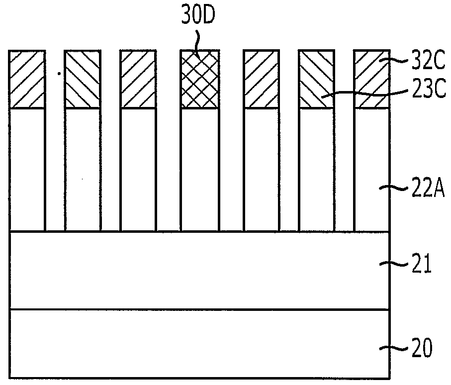
[0027]Embodiments of the present invention relate to a method for forming a fine pattern using a quadruple patterning in a semiconductor device. In the embodiments of the present invention, pattern fidelity and space uniformity may be secured because a spacer patterning is not repeatedly performed on one partition pattern.

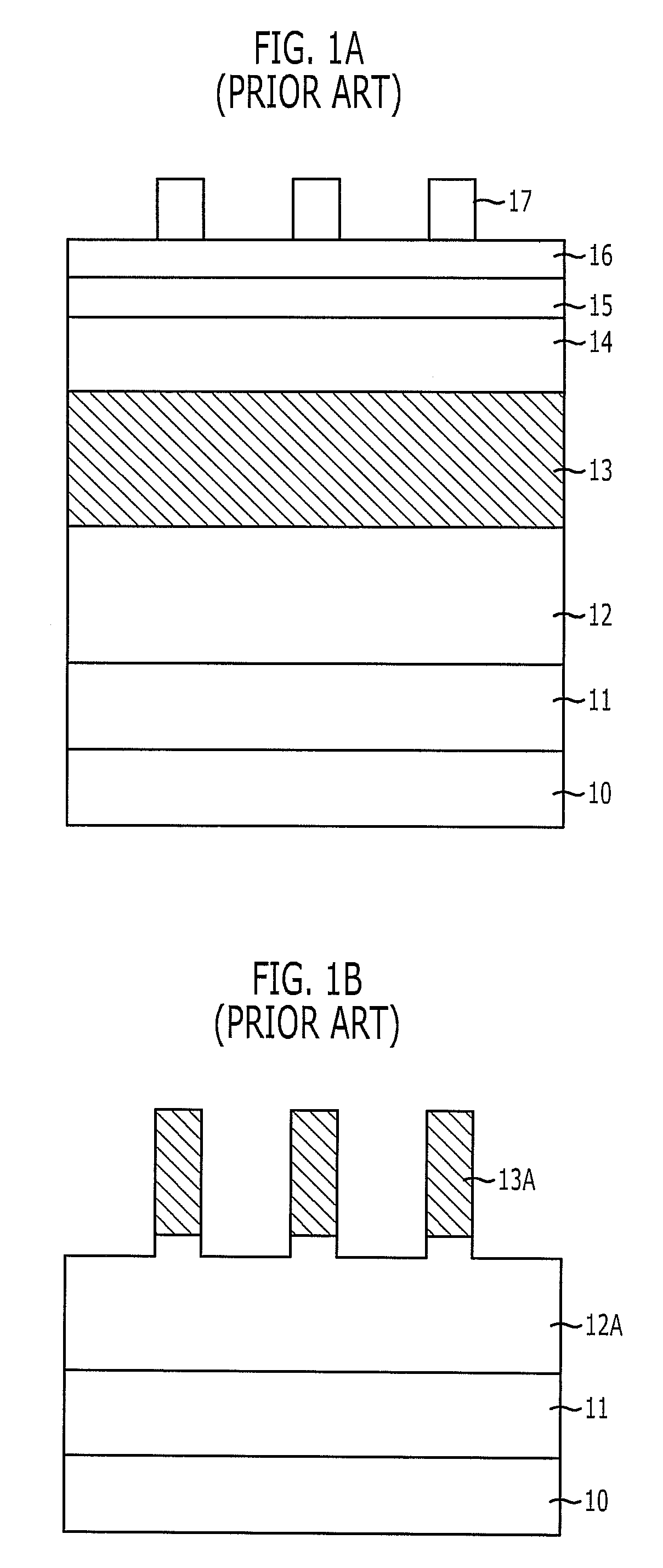
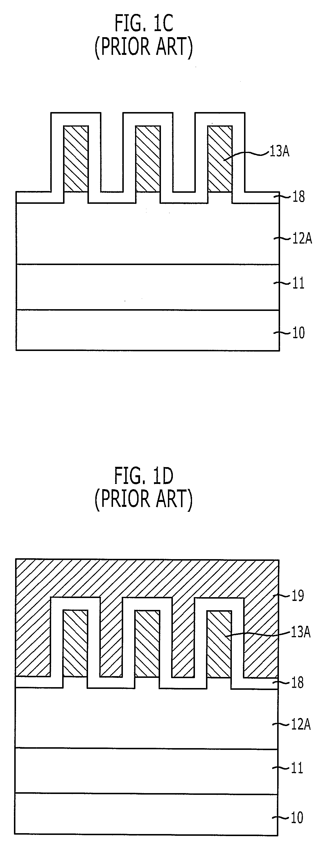
[0028]Meanwhile, a critical dimension (CD) of a partition pattern may be large when etching a partition layer to form a first partition in accordance with the embodiments of the present invention. According to a typical method, it is difficult to have a large CD for a partition pattern considering the thickness of a spacer oxide layer because the spacer oxide layer is additionally formed after the partition pattern is formed. However, in accordance with the embodiments of the prese...


PUM


Abstract

A method for forming a fine pattern in a semiconductor device using a quadruple patterning includes forming a first partition layer over a first material layer which is formed over a substrate, performing a photo etch process on the first partition layer to form a first partition pattern, performing an oxidation process to form a first spacer sacrificial layer over a surface of the first partition pattern, forming a second spacer sacrificial layer over the substrate structure, forming a second partition layer filling gaps between the first partition pattern, removing the second spacer sacrificial layer, performing an oxidation process to form a third spacer sacrificial layer over a surface of the second partition layer and define a second partition pattern, forming a third partition pattern filling gaps between the first partition pattern and the second partition pattern, and removing the first and third spacer sacrificial layers.

Description

CROSS-REFERENCE TO RELATED APPLICATIONS[0001]The present invention claims priority of Korean patent application number 10-2008-0138590, filed on Dec. 31, 2008, the disclosure of which is incorporated herein by reference in its entirety.BACKGROUND OF THE INVENTION[0002]The present invention relates to a method for fabricating a semiconductor device, and more particularly, to a method for forming a fine pattern in a semiconductor device using a quadruple patterning.[0003]As semiconductor devices are continuously becoming highly integrated, micronization of various patterns, e.g., lines and space patterns, needed for forming circuits constituting a semiconductor device is accelerating.[0004]However, there are limitations as to the micronization of patterns due to limitations of photolithography equipments, in particular, photo-exposure equipments. It is difficult for the current photo-exposure equipments to form a fine pattern having a line width smaller than 40 nm due to resolution li...

Claims


Application Information

Patent Timeline
Patent Type & Authority Applications(United States)
IPC IPC(8): H01L21/306
CPCH01L21/0337H01L21/0338G03F7/70466H01L21/31116
Inventor KIM, WON-KYU
Owner SK HYNIX INC
Why Eureka
Try Eureka