Electronic device and method of controlling a communication

a communication and electronic device technology, applied in the direction of digital computers, multi-programming arrangements, instruments, etc., can solve the problems of increasing the complexity of the control system of the hardwired components in the actual silicon prototype/product, the inability to accurately determine up-front when key on-chip events occur, and the complexity of the functionality of the electronic circuit or integrated circuit (ic). to achieve the effect of improving the control of the communication within the electronic devi

Inactive Publication Date: 2010-07-01
KONINKLIJKE PHILIPS ELECTRONICS NV
View PDF8 Cites 6 Cited by
  • Summary
  • Abstract
  • Description
  • Claims
  • Application Information

AI Technical Summary

Benefits of technology

[0004]It is an object of the invention to provide an electronic device with improved control over the communication within the electronic device.
[0017]The invention relates to the idea to take advantage of the convergence of hardware and software co-design. At the highest abstraction level of hardware design, components of an electronic device are communicating to each other via high-level data representations, called transactions, i.e. transaction level. At the lowest level of software design abstraction, i.e. where software has been mapped onto the programmable components of the system, again transaction-level models are used to analyze, verify, and tune the application software. This makes the transaction-level the common denominator for both software and hardware designers, such that software and hardware engineers can share the same view of the actual behavior of the system, enhancing the localization of any remaining hardware and software errors or inefficiencies. This in turn leads to a significant reduction in time-to-market and, when properly fed back to the design community, tools and flows, to an improvement of the product creation process.

Problems solved by technology

Within recent years, electronic circuits or Integrated Circuits (ICs) have become increasingly more complex with respect to their functionality, their number of programmable components, and their communication.
The implementation of control systems for hardwired components in actual silicon prototypes / products is more difficult as it has to be established prior to IC manufacturing where to put what breakpoints.
In addition, these systems often exhibit run-time data-dependent behavior, making it extremely difficult, if not impossible, to accurately determine up-front when key on-chip events occur.

Method used


Image

  • Electronic device and method of controlling a communication
  • Electronic device and method of controlling a communication
  • Electronic device and method of controlling a communication

Examples


Embodiment Construction

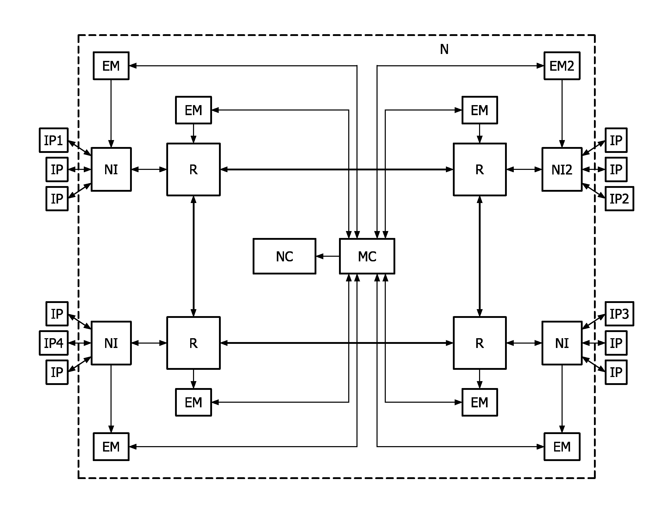
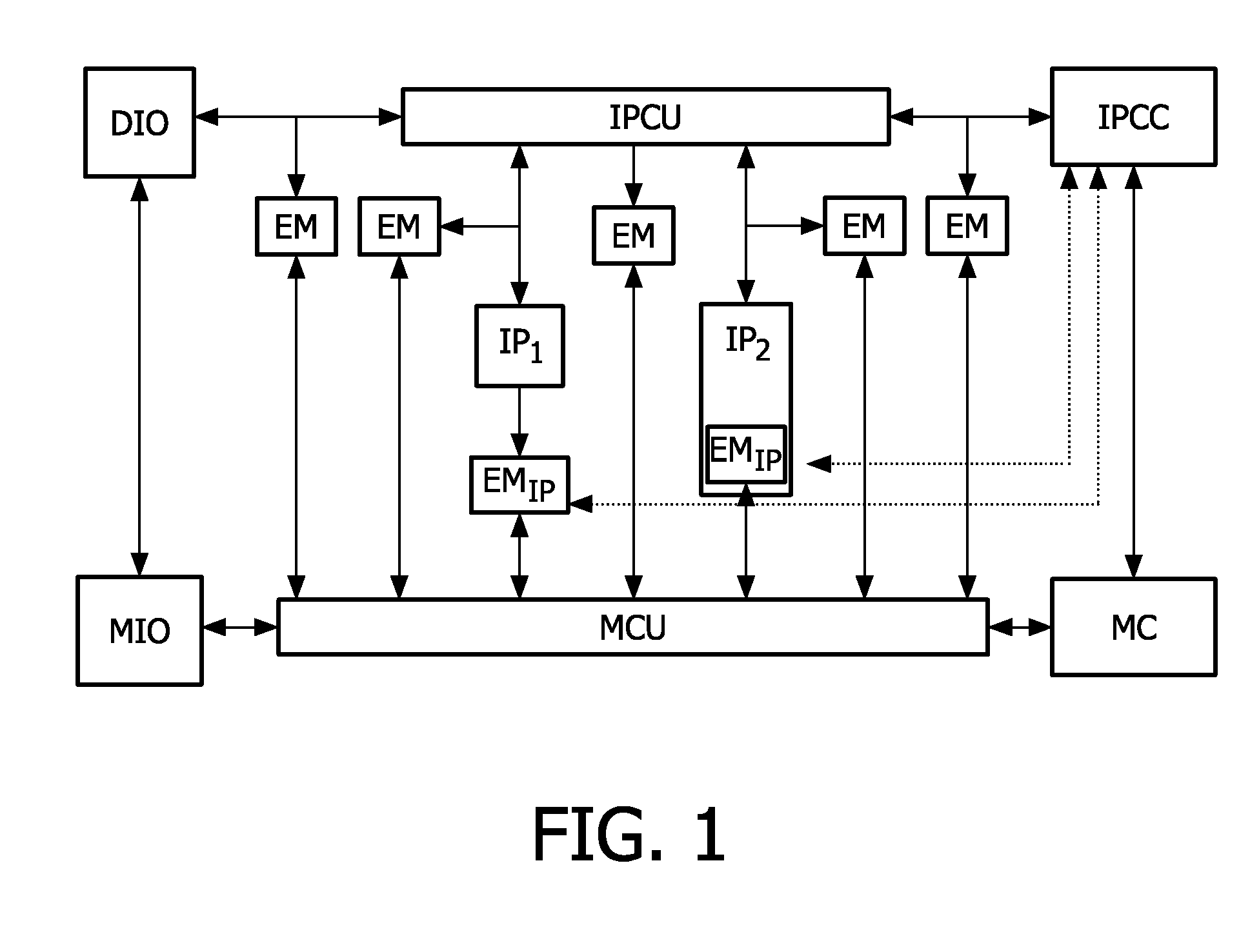
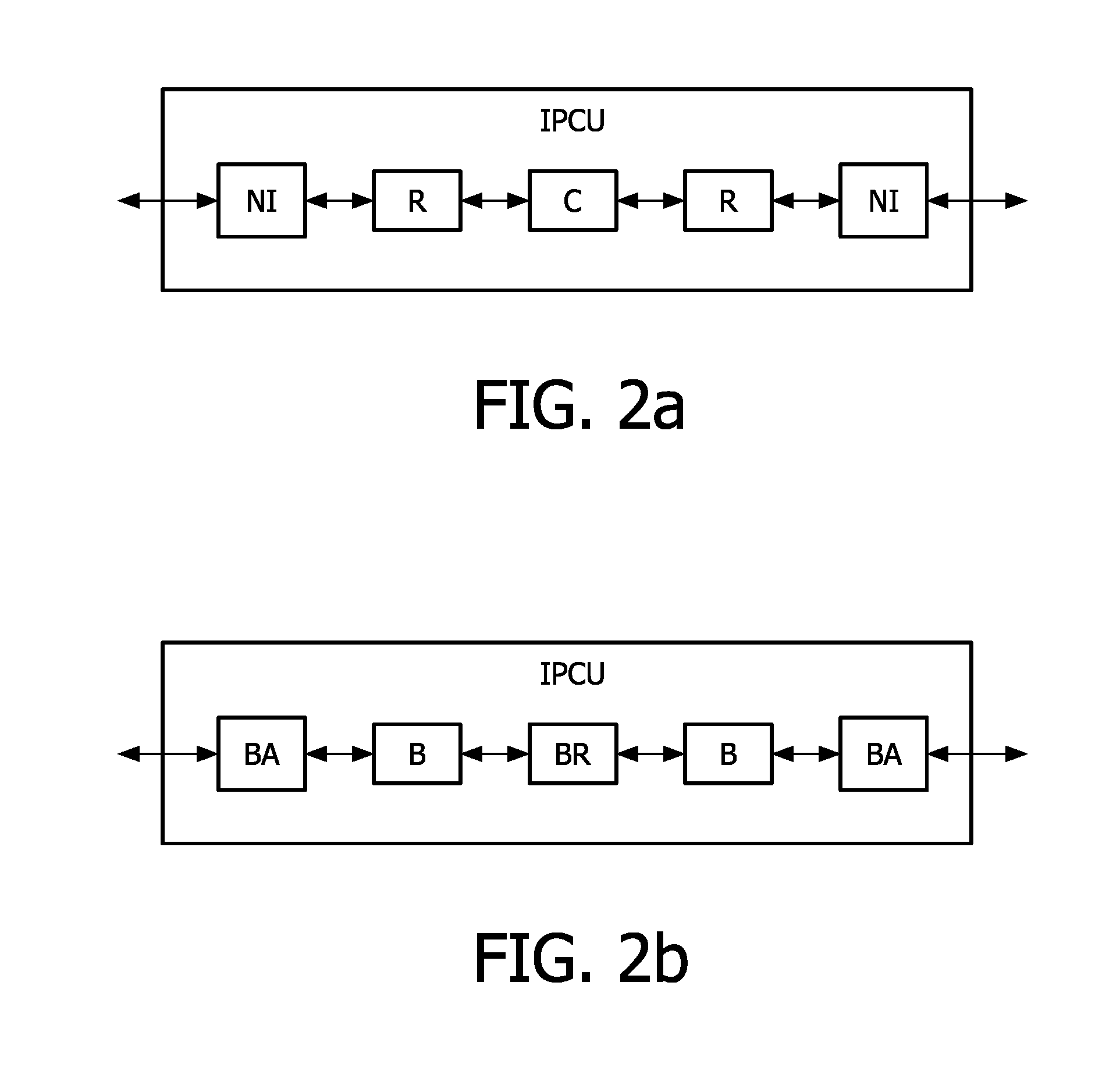
[0025]FIG. 1 shows a block diagram of an architecture of an embodiment of a system on chip according to the present invention. The system on chip comprises a plurality of intellectual property IP blocks IP which communicate with each other by an IP communication unit IPCU which may serve as an interconnect. The communication unit IPCU may be implemented as a single homogenous interconnect (e.g. routers or busses and bridges) or may comprise multiple heterogeneous interconnects (e.g. physically: switches, busses, routers, bridges, high speed, low speed or logically: data, control interrupt, debug and power management interconnects). An IP communication controller IPCC controls the traffic between the IP blocks IP via the IP communication unit IPCU. The IP communication controller IPCC can be implemented as a centralized controller or as distributed controllers. The system on chip according to the invention may be implemented on a single die or chip or may extend over multiple dies or...


PUM


Abstract

An electronic device is provided which comprises a plurality of processing units (IP; IP1-IP4), an interconnect (IPCU; N) for coupling the processing units (IP; IP1-IP4) to enable a communication between the processing units (IP; IP1-IP4) and at least one event monitor (EM) for detecting events in the communication in the electronic device. The electronic device furthermore comprises a first controller unit for controlling the interconnect (IPCU; N) according to one or more of the events detected by the at least one event monitor (EM).

Description

FIELD OF THE INVENTION[0001]The present invention relates to an electronic device and a method of controlling the communication in an electronic device.BACKGROUND OF THE INVENTION[0002]Within recent years, electronic circuits or Integrated Circuits (ICs) have become increasingly more complex with respect to their functionality, their number of programmable components, and their communication. Therefore, the complexity of software and hardware (co-) design increases accordingly and an efficient verification, debug, and optimization is required.[0003]In the design and manufacturing of state-of-the-art ICs, including ASIC, ASSP, FPGA, PLD, CPLD and structured ASIC devices, the control of digital programmable components upon user-interaction or (a sequence of) events is enabled and heavily exploited in (software and hardware) design verification and silicon debug. In www.arm.com / products / solutions / CoreSight.html, control systems are shown that are able to handle single or multiple progr...

Claims


Application Information

Patent Timeline
Patent Type & Authority Applications(United States)
IPC IPC(8): G06F15/80G06F9/06G06F9/46G06F13/14
CPCG06F11/3636G06F11/3648
Inventor BENNEBROEK, MARTINUS THEODORUSGOOSSENS, KEES GERARD WILLEMVERMEULEN, HUBERTUS GERARDUS HENDRIKUS
Owner KONINKLIJKE PHILIPS ELECTRONICS NV
Why Eureka
Try Eureka