Conductive film and manufacturing method thereof, and transparent electromagnetic shielding film

a technology of electromagnetic shielding film and conductive film, which is applied in the field of transparent and conductive electromagnetic shielding film for plasma display, can solve the problems of increasing electromagnetic interference (emi), affecting the operation of such a device, and causing malfunction, and achieves the effects of small change in color taste with time, good adhesion, and hardly peeling of the blackening layer

Active Publication Date: 2010-07-08
FUJIFILM CORP
View PDF10 Cites 12 Cited by
  • Summary
  • Abstract
  • Description
  • Claims
  • Application Information

AI Technical Summary

Benefits of technology

[0219]For the purpose of forming the conductive metal layer inexpensively and easily, it is preferred to apply silver development. In order to achieve this, the amount of silver is preferably 0.05 g / m2 or more; and when the amount of silver is more than 2.0 g / m2, the light transmission properties are lowered and the costs are not cheap, and therefore, such is not preferable. Copper is preferable because it is cheap and is able to lower the surface resistivity. When the amount of copper is less than 0.2 g / m2, a preferred surface resistivity value is not obtainable, whereas when it exceeds 5.0 g / m2, the light transmission properties are lowered and the haze becomes large, and therefore, such is not preferable. When the mass ratios of nickel and zinc fall within the ranges of the invention, the effects of the invention are obtainable. When the amount of nickel or zinc is less than 0.06 g / m2, the change of color taste after elapsing becomes large, and therefore, such is not preferable. On the other hand, when the amount of nickel or zinc exceeds 2.0 g / m2, the adhesion of the blackening layer is deteriorated and the light transmission properties are lowered, and therefore, such is not preferable.
[0220]It is especially preferable that the conductive metal layer in a pattern-like state is a laminated constitution of two layers of silver and copper obtained by adjusting an applied voltage and a composition of the electrolytic solution such that copper is selectively electrodeposited on an upper surface of mesh-like developed silver (surface in an opposite side to the support); and that plating is performed such that the silver layer is positioned in the support side, thereby additionally providing a blackening layer.
[0221]A width of the mesh line after performing up to the blackening treatment is preferably from 5 to 30 μm, and more preferably from 8 to 20 μm. A pitch interval of the mesh is preferably from 50 to 600 μm, and especially preferably from 100 to 400 m. In order to enhance the light transmittance, it is preferable that the light width is thin and that the pitch interval is wide. Since the electromagnetic shielding ability is in a trade-off relationship, the foregoing optimum range is determined. The line width may be uniform; points of intersection may be thick; and inversely, points of intersection may be thin, with a central part of the line between the points of intersection being thick. In the case of using the conductive metal layer as an electromagnetic shielding film for PDP, the lattice-like pattern of the mesh has an angle against the end faces of the film of from 30 to 70°, and especially preferably from 40 to 65°. Instead of the lattice-like pattern, the mesh can also take a radial form such as a cobweb. In all of these cases, it is required that the blackening layer of the invention be present.
[0222]Next, the blackening layer forming step of the invention is described. The blackening layer forming step is to form a blackening layer having a mass ratio of nickel and zinc of the blackening layer satisfied with the following formula (1) on the foregoing plating layer (conductive metal layer) by using a plating liquid containing nickel and zinc.Ni:Zn=0.5:1 to 50:1  (1)
[0223]It is preferable that in the blackening layer forming step, the foregoing blackening layer is formed in two or more stages by using a first blackening plating liquid containing nickel and zinc and a second blackening plating liquid containing nickel and zinc, with a content ratio of nickel in the first placing liquid being larger than a content ratio of nickel in the foregoing second plating liquid. At this time, the blackening layer is composed of two or more layers. With respect to the blackening layer composed of two or more layers, in the blackening layer of a surface layer, the zinc content is larger than the content of nickel.
[0224]In the case where the blackening layer is formed in two or more stages, from the viewpoint of suppressing the poor appearance, a content molar ratio of nickel and zinc of the foregoing first plating liquid is preferably satisfied with the following formula (2), and more preferably satisfied with the following formula (2-a).Ni:Zn=10:1 to 100:1  (2)Ni:Zn=20:1 to 60:1  (2-a)

Problems solved by technology

In recent years, following an increase in utilization of various electrical equipment and electronic application equipment, electromagnetic interference (EMI) increases rapidly.
It is pointed out that EMI not only becomes a cause of malfunction or interference of electronic or electric appliances but also gives health interference to an operator of such a device.
Thus, these methods are often inadequate as an electromagnetic shielding method to be applied to display appliances.
Accordingly, there is involved a problem that not only light from the outside of the panel is reflected, whereby the contrast of the screen is deteriorated, but also the reflected color of the copper foil is viewed.
Furthermore, there is involved a problem that light emitted within the screen is reflected, too, whereby the image display quality of the display panel is deteriorated.
If it is intended to apply this as an electromagnetic shielding film for PDP, discoloration with time is large, and therefore, such was problematic.

Method used


Image

  • Conductive film and manufacturing method thereof, and transparent electromagnetic shielding film
  • Conductive film and manufacturing method thereof, and transparent electromagnetic shielding film

Examples


embodiment

[0291]The invention is more specifically described below with reference to the following Examples. Incidentally, materials, use amounts, proportions, treatment contents, treatment procedures, and so on shown in the following Examples can be properly altered so far as the gist of the invention is not deviated. Accordingly, it should not be construed that the scope of the invention is limited by the following specific examples.

example 1

Preparation of Silver Halide Photosensitive Material

[0292]An emulsion containing 10.0 g of gelatin based on 60 g of Ag in an aqueous medium and containing a silver iodobromochloride grain (I=0.2% by mole, Br=40% by mole) having a sphere-corresponding average grain size of 0.1 μm was prepared.

[0293]Also, K3Rh2Br9 and K2IrCl6 were added in this emulsion in a concentration of 10−7 (mole / mole of Ag), thereby doping the silver bromide grain with an Rh ion and an Ir ion. Na2PdCl4 was added in this emulsion, and the mixture was subjected to gold-sulfur sensitization with chloroauric acid and sodium thiosulfate. Thereafter, the resulting emulsion was coated together with a gelatin film-hardener in a coating amount of silver of 1 g / m2 on a support made of polyethylene terephthalate (PET). On that occasion, an Ag / gelatin volume ratio was set up at 1 / 2.

[0294]The PET support used had a thickness of 90 μm and a width of 30 cm. The emulsion was coated in a width of 25 cm on the PET support having...

example 2

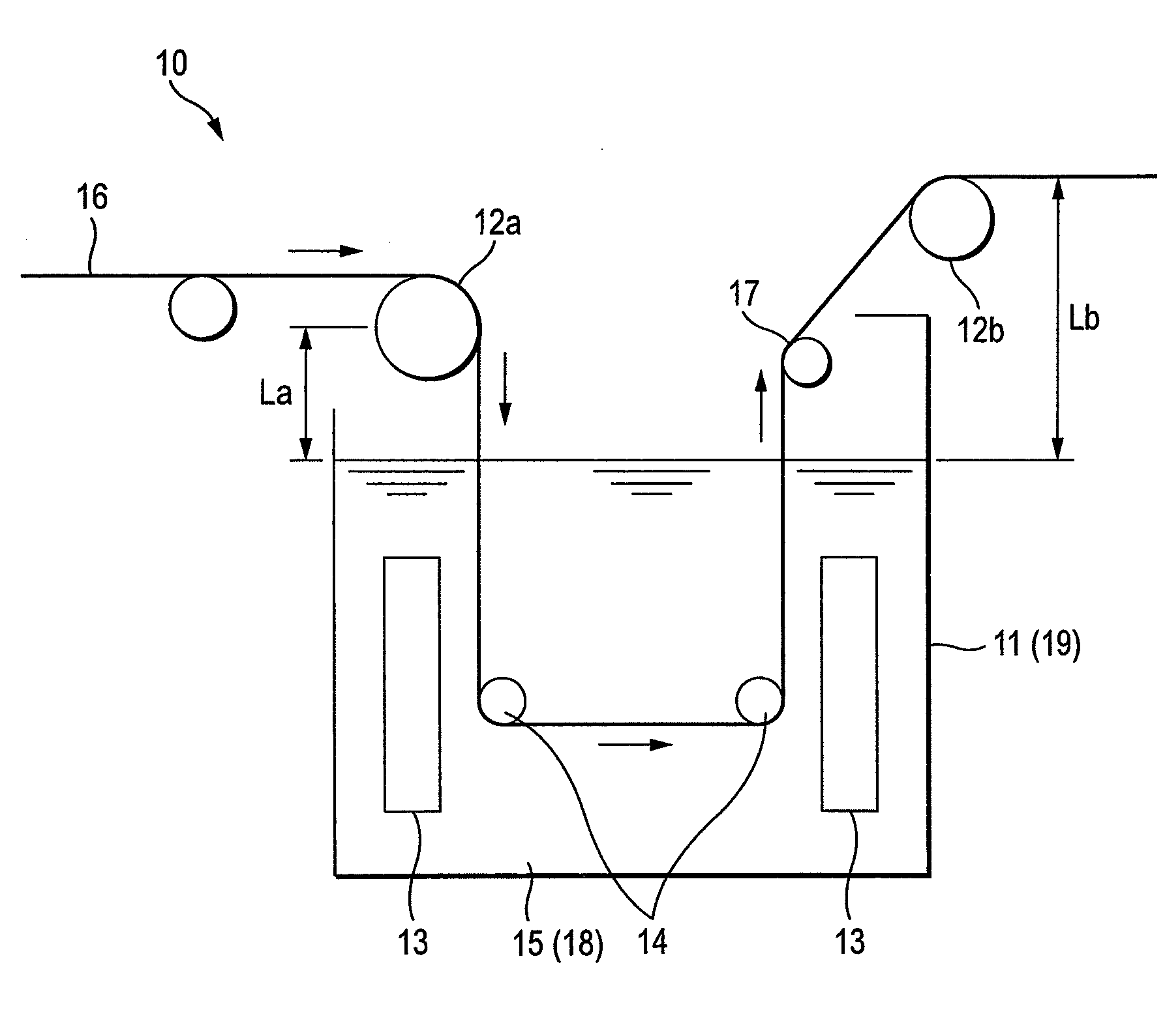
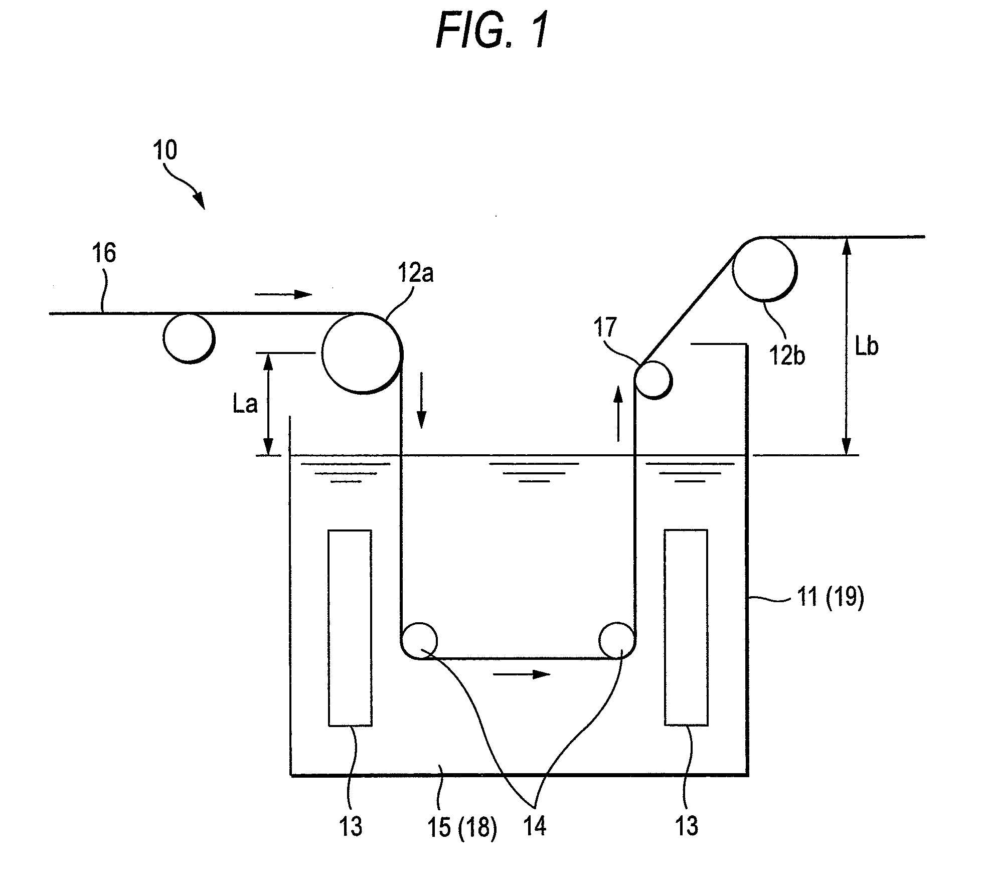
[0329]Under the condition of Ni:Zn=7:1 in Example 1, the treatment was carried out by changing the anode of the blackening tank from the carbon electrode to a nickel electrode (by using 0.1N sulfuric acid for the pH adjustment) and using the following blackening liquid. As a result, defect and unevenness of the metal mesh film and staining by a transparent deposit were not observed at all; and in addition, the white stain of the film edge as observed in Example 1 was not observed at all.


PUM

PropertyMeasurementUnit
mass ratioaaaaaaaaaa

Abstract

An electromagnetic shielding film for plasma display which is excellent in electromagnetic shielding characteristics for effectively shielding electromagnetic waves, near infrared rays, stray light, external light, and the like and even when stored under a wet heat condition, is small in change of color tint and good in adhesion, with a blackening layer hardly peeled away, is provided by a transparent electromagnetic shielding film including a transparent support having thereon a conductive metal layer in a pattern-like state having an electromagnetic shielding ability and having a surface covered by a blackening layer, with the blackening layer made of an alloy of nickel and zinc in a nickel / zinc mass ratio of from 0.5 to 50.

Description

TECHNICAL FIELD[0001]The present invention relates to a conductive film and a method of manufacturing the same and to a transparent electromagnetic shielding film. Above all, the invention relates to a transparent and conductive electromagnetic shielding film for plasma display, which even when stored under a wet heat condition, is small in change of color tint and good in adhesion and which is prepared by applying a plating treatment.BACKGROUND ART[0002]In recent years, following an increase in utilization of various electrical equipment and electronic application equipment, electromagnetic interference (EMI) increases rapidly. It is pointed out that EMI not only becomes a cause of malfunction or interference of electronic or electric appliances but also gives health interference to an operator of such a device. For that reason, in electronic or electric appliances, it is required that the intensity of electromagnetic wave discharge is controlled within the standards or regulations...

Claims


Application Information

Patent Timeline
Patent Type & Authority Applications(United States)
IPC IPC(8): H05K9/00G03F7/20
CPCB32B15/08H05K9/0096B32B7/025
Inventor SASAKI, HIROTOMOMATSUMOTO, JUNYAMAZAKI, TAKAYASUHAIJIMA, AKIMITSUFUJITA, YOSHIHIRO
Owner FUJIFILM CORP
Why Eureka
Try Eureka