Multilayer substrate and method of manufacturing the same

a technology of multi-layer substrates and manufacturing methods, applied in the direction of final product manufacturing, dielectric characteristics, conductive pattern formation, etc., can solve the problems of limiting the movement of electronic elements, affecting the bending angle of electronic elements, etc., to achieve the effect of large bending angl

Active Publication Date: 2010-07-15
MURATA MFG CO LTD
View PDF9 Cites 8 Cited by
  • Summary
  • Abstract
  • Description
  • Claims
  • Application Information

AI Technical Summary

Benefits of technology

[0013]In the present manufacturing method, when the electric element is inserted in the through hole, the protruding member pressed by the electric element may bend from the spacer as a supporting point with a large bending angle. Thereby, even when the electric element is out of position with respect to the through hole, the electric element is pushed toward a center portion of the through hole by a reaction force from the protruding members before the protruding members receive a force over a break strength of the protruding members. As a result, the present manufacturing method restricts a generation of a resin dust due to inserting of the electric element.

Problems solved by technology

Thus, the electronic element is restricted from displacing during a manufacturing process.
According experiments by the inventor of the present application, in a case where the electronic element is out of position with respect to the through hole when the electronic element is inserted in the through hole, the electronic element may chip off the protruding members and may generate a resin dust.
In contrast, in a case where the electronic element is positioned with respect to the through hole with a high accuracy, it may take a long time to inserting the electronic element.
Thus, the positioning of the electric element with a high accuracy is unsuitable for a case where a plurality of electronic elements is inserted in a multilayer substrate.

Method used


Image

  • Multilayer substrate and method of manufacturing the same
  • Multilayer substrate and method of manufacturing the same
  • Multilayer substrate and method of manufacturing the same

Examples


first embodiment

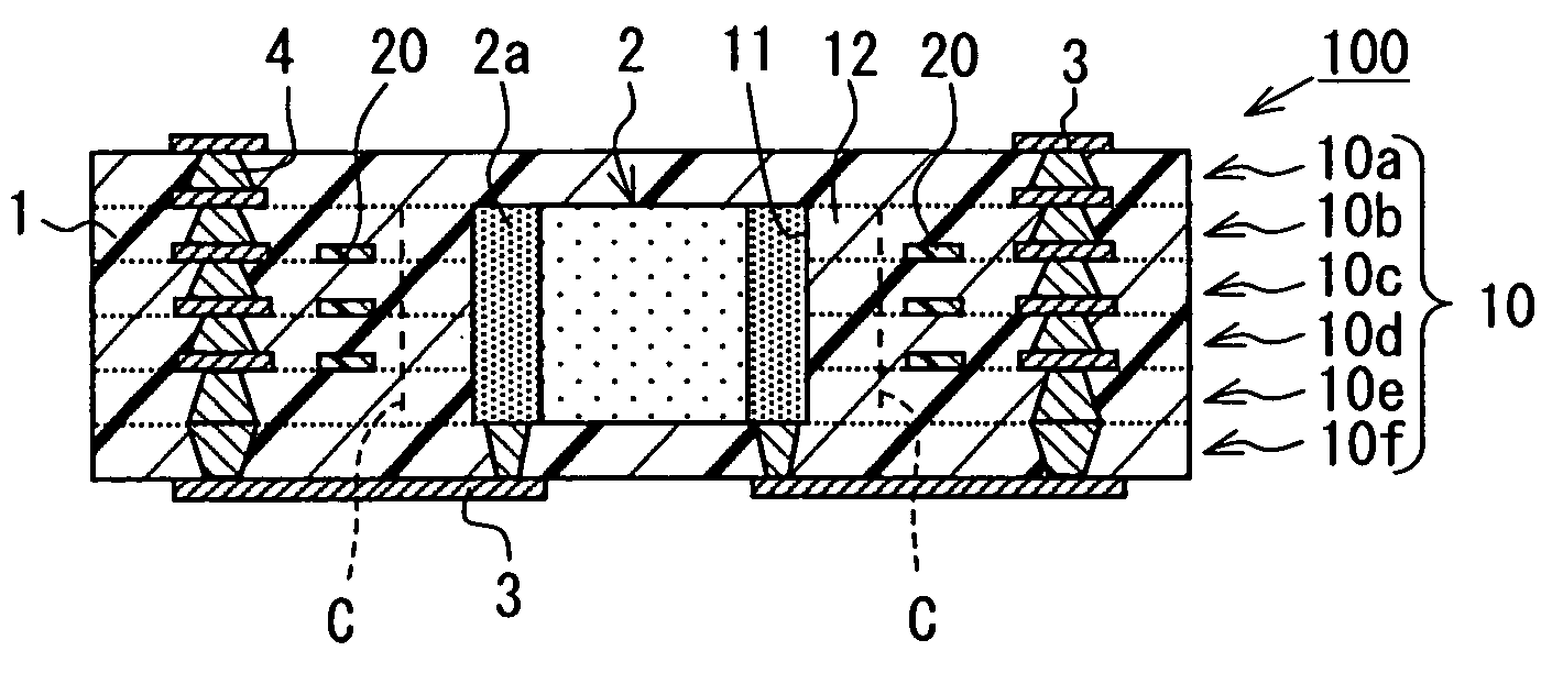
[0041]As shown in FIG. 4, a multilayer substrate 100 includes an insulating base member 1 and an electric element 2 embedded in the insulating base member 1. The insulating base member 1 includes a plurality of resin films 10 attached each other. For example, the resin films 10 includes six resin films 10a to 10f having a thermal plasticity and arranged in order from top to bottom. The multilayer substrate 100 also includes conductive patterns 3 having a multilayer structure and coupled with each other through conductive members 4. The conductive members 4 are made of a sintered conductive paste. The electronic element 2 has electrodes 2a coupled with the conductive patterns 3 through the conductive members 4. In the six resin films 10a to 10f, four resin films 10b to 10e arranged between a top resin film 10a and a bottom resin film 10f have a through hole 11, for inserting the electric element 2. Each of the four resin films 10b to 10d has a plurality of protruding members 12 protr...

second embodiment

[0059]In the multilayer substrate 100 in FIG. 4, the material of the spacers 20 is different with those of other components in the multilayer substrate 100. Alternatively, the spacers 20 may be made of the same material as one of the other components.

[0060]For example, as shown in FIG. 14, spacers 21 made of the same thermoplastic resin (e.g., liquid crystal polymer) as the films 1a may be used as the spacers 20. The spacers 21 are formed by punching of a thermoplastic resin film, which is thinner than the films 1a. The spacers 21 have similar shapes with those of the spacers 20.

[0061]In a case where the spacers 21 and the films 1a are made of the same material, when the resin films 10a to 10f are attached to each other to form the insulating base member 1 in the heating and pressing process, the spacers 21 are also softened and attach to adjacent films 10, as shown in FIG. 15. Thus, a connection reliability between the spacers 21 and the resin films 10 increases.

[0062]In addition, ...


PUM

PropertyMeasurementUnit
conductiveaaaaaaaaaa
friction coefficientaaaaaaaaaa
bending angleaaaaaaaaaa

Abstract

A multilayer substrate includes an insulating base member having a plurality of resin films, an electric element embedded in the insulating base member, and a spacer. The resin films are made of a thermoplastic resin and stacked and attached to each other. At least one resin film has a through hole for inserting the electric element. The one resin film further has a plurality of protruding members. One protruding member opposes to another one protruding member so that the one and the another one contact and sandwich the electric element. The spacer is arranged between the one resin film and an adjacent resin film and is disposed at a base portion of one of the protruding members.

Description

CROSS REFERENCE TO RELATED APPLICATION[0001]This application is based on Japanese Patent Application No. 2006-329856 filed on Dec. 6, 2006, the content of which is incorporated herein by reference in its entirety.BACKGROUND OF THE INVENTION[0002]1. Field of the Invention[0003]The present invention relates to a multilayer substrate and a method of manufacturing the same.[0004]2. Description of the Related Art[0005]US 2006 / 0042078 A (corresponding to JP 2006-73763 A) discloses a manufacturing method of a multilayer substrate that includes an insulating base member and an electronic element embedded in the insulating base member. In the manufacturing method, the insulating base member includes a plurality of resin films and a part of the resin films has a through hole, in which the electric element is inserted. At least one of the resin films having the through hole is provided with a plurality of protruding members. The protruding members protrude from surrounding portions of the thro...

Claims


Application Information

Patent Timeline
Patent Type & Authority Applications(United States)
IPC IPC(8): H05K3/10
CPCH05K1/183Y10T29/49126H05K3/4614H05K3/4617H05K3/4632H05K2201/0129H05K2201/091H05K2201/09781H05K2201/09909H05K2201/1059H05K2201/10636H05K2201/2036H05K2203/063Y10T29/4913Y10T29/49155Y10T29/49128H05K1/186Y02P70/50
Inventor KAMIYA, HIROKISHIMIZU, MOTOKITAKEUCHI, SATOSHI
Owner MURATA MFG CO LTD
Why Eureka
Try Eureka