Information processing device that accesses memory, processor and memory management method

a technology of information processing device and memory, applied in the direction of memory adressing/allocation/relocation, digital storage, instruments, etc., can solve the problems of inability to maintain the contents of the main memory, the content of the main memory is lost, and the execution time is long

Inactive Publication Date: 2010-07-22
TOSHIBA MEMORY CORP
View PDF5 Cites 31 Cited by
  • Summary
  • Abstract
  • Description
  • Claims
  • Application Information

AI Technical Summary

Benefits of technology

[0011]An information processing device of a first example of the invention comprises: an address generation section that generates a write address indicating a write position in a nonvolatile memory so that the write position is shifted in order to suppress each number of times of overlapped writing for each position of the nonvolatile memory when a write operation to the nonvolatile memory from a processor is performed; an order generation section that generates order information indicating a generation order of the writing operation; and a write control section that stores write information to the write address generated by the address generation section, and stores the order information to the nonvolatile memory so that the order information is related to at least one of the stored write information and the write address.

Problems solved by technology

In the conventional information processing device, the contents of the main memory are lost if the power source thereof is turned off.
Therefore, in the conventional information processing device, the boot operation of a system is required at each boot time, it is required to move a program or data from the secondary memory device to the main memory for program starting or data reading and it takes a long time for execution.
Further, in the conventional information processing device, the contents of the main memory cannot be maintained if the power source thereof is turned off.
Therefore, when the conventional information processing device is not correctly shut down, there occurs a possibility that data, a system or program will be destroyed.

Method used


Image

  • Information processing device that accesses memory, processor and memory management method
  • Information processing device that accesses memory, processor and memory management method
  • Information processing device that accesses memory, processor and memory management method

Examples


first embodiment

[0026]In an information processing device according to the present embodiment, a nonvolatile main memory (main storage device) is utilized for a processor.

[0027]Even when the processor uses the nonvolatile main memory for an application different from an application for a main memory, the same access control operation can be used.

[0028]In this embodiment, for example, it is supposed that the information processing device includes a processor such as a micro processing unit (MPU) or the processor and a memory.

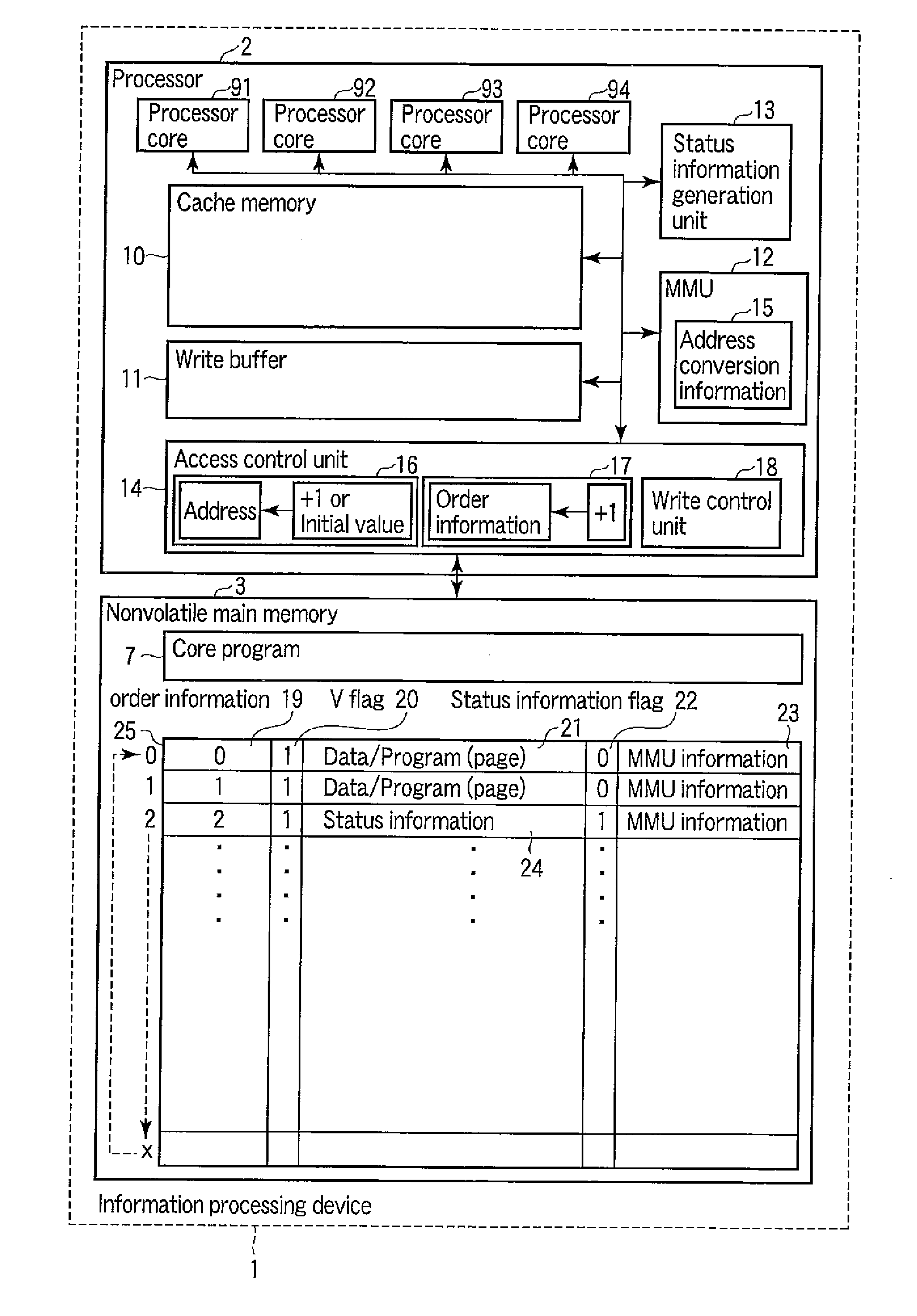
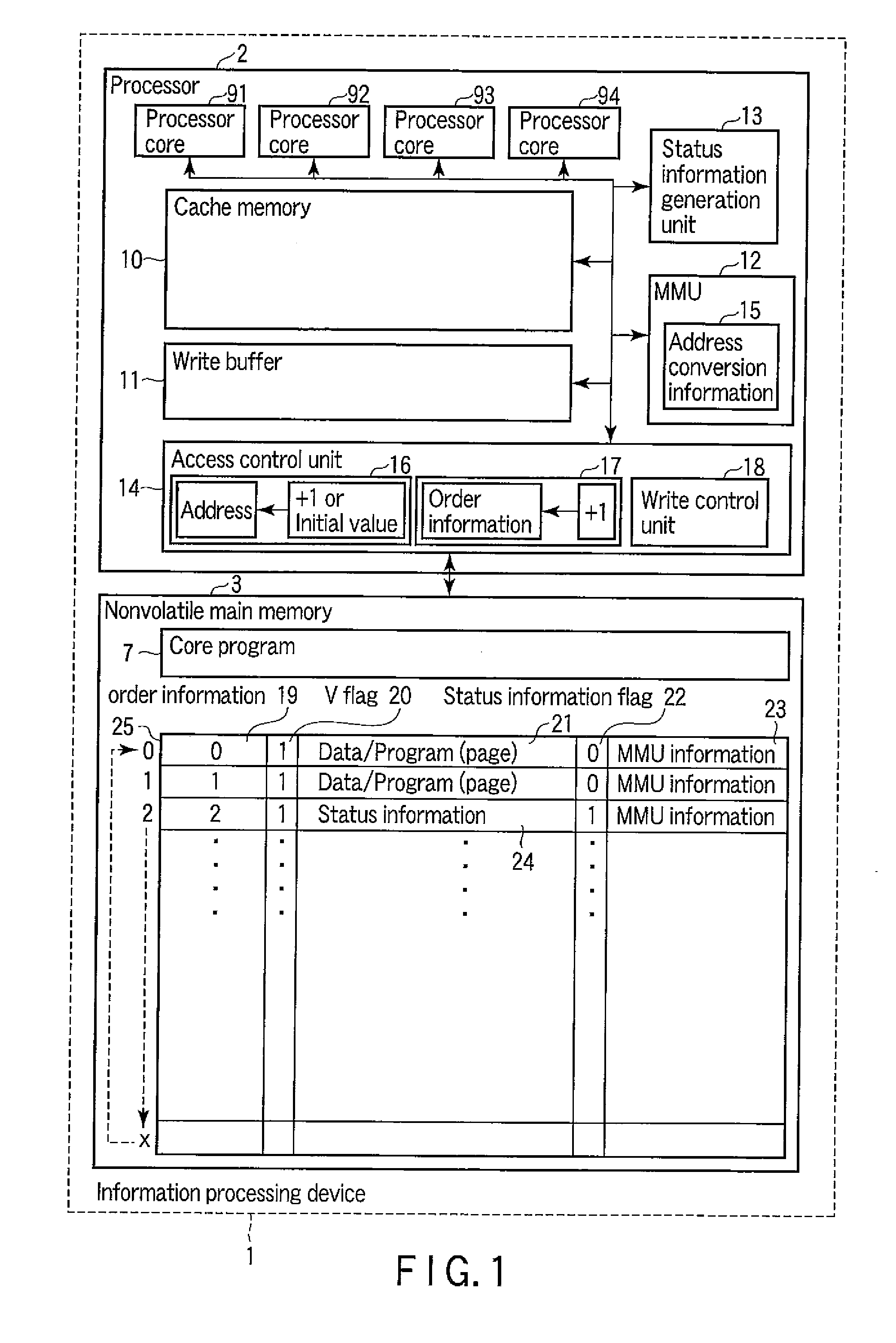
[0029]FIG. 1 is a block diagram showing one example of a detailed configuration of the information processing device according to this embodiment.

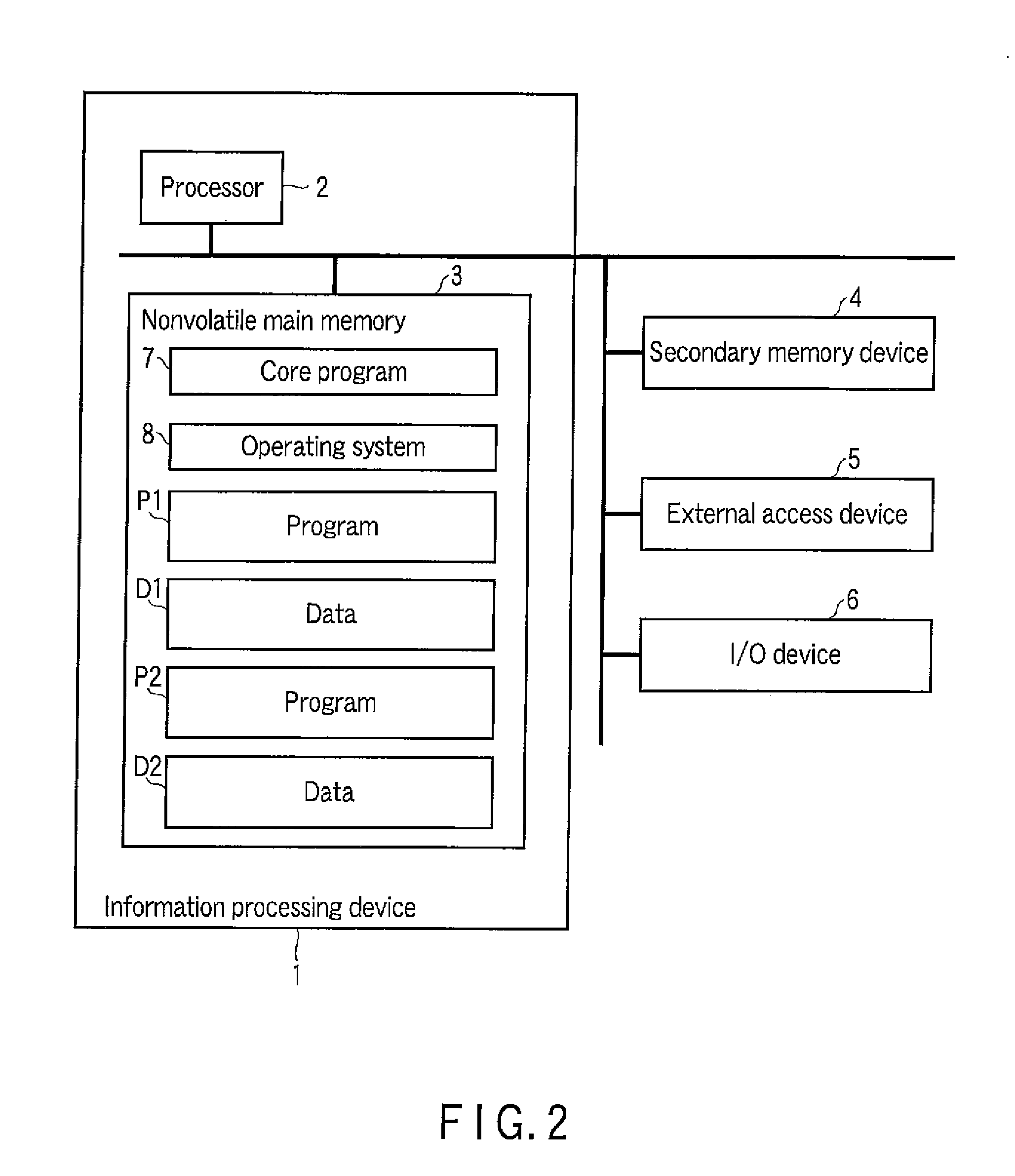
[0030]Further, FIG. 2 is a block diagram showing one example of a schematic configuration of the information processing device according to this embodiment.

[0031]An information processing device 1 includes a processor 2 and nonvolatile main memory 3. The processor 2 can access various devices such as a secondary memory (storage) device...

second embodiment

[0108]In this embodiment, an information processing device that is a modification of the information processing device 1 according to the first embodiment and has a configuration in which the cache memory is formed in a hierarchical form is explained.

[0109]FIG. 6 is a block diagram showing one example of a configuration of an information processing device according to this embodiment.

[0110]An information processing device 26 includes at least one processor (four processors in the example shown in FIG. 6) 271 to 274, control device 28 and nonvolatile main memory 3. The information processing device 26 can access other devices, for example, the secondary memory device 4, external access device 5, I / O device 6 and the like.

[0111]The respective processors 271 to 274 include primary cache memories 291 to 294. When cache miss occurs in the primary cache memories 291 to 294, the processors 271 to 274 transmit a to-be-accessed address (access target address) to the control device 28.

[0112]T...

third embodiment

[0114]In this embodiment, a case wherein a writing number check unit and abnormality detection unit are added to the information processing device according to the first or second embodiments is explained. In this example, a case wherein a writing number check unit and abnormality detection unit are added to the information processing device 1 according to the first embodiment is explained in the present embodiment, but this can be similarly applied to another information processing device according to another embodiment, for example, the information processing device 26 according to the second embodiment.

[0115]FIG. 7 is a block diagram showing one example of a configuration of an information processing device according to this embodiment.

[0116]A memory management unit 32 of a processor 31 of an information processing device 30 according to this embodiment comprises writing number information 33 indicating the number of times of write operations and Bad information 34 for each area ...


PUM


Abstract

An information processing device of an example of the invention comprises an address generation section that generates a write address indicating a write position in a nonvolatile memory so that the write position is shifted in order to suppress each number of times of overlapped writing for each position of the nonvolatile memory when a write operation to the nonvolatile memory from a processor is performed, an order generation section that generates order information indicating a generation order of the writing operation, and a write control section that stores write information to the write address, and stores the order information to the nonvolatile memory so that the order information is related to at least one of the stored write information and the write address.

Description

CROSS-REFERENCE TO RELATED APPLICATIONS[0001]This application is based upon and claims the benefit of priority from prior Japanese Patent Application No. 2009-008079, filed Jan. 16, 2009, the entire contents of which are incorporated herein by reference.BACKGROUND OF THE INVENTION[0002]1. Field of the Invention[0003]The present invention relates to an information processing device that accesses a memory, processor, and memory management method.[0004]2. Description of the Related Art[0005]In the conventional information processing device, a volatile memory such as a dynamic random access memory (DRAM), for example, is used as a main memory of a processor. Further, in the conventional information processing device, a secondary memory (storage) device is used in combination with the volatile memory.[0006]In the conventional information processing device, the contents of the main memory are lost if the power source thereof is turned off. Therefore, in the conventional information proces...

Claims


Application Information

Patent Timeline
Patent Type & Authority Applications(United States)
IPC IPC(8): G06F12/02G06F12/00
CPCG06F12/0246G06F12/0866G06F2212/2022G06F2212/7201
Inventor OMIZO, TAKASHIKUNIMATSU, ATSUSHI
Owner TOSHIBA MEMORY CORP
Why Eureka
Try Eureka