Solid-state image sensor and drive method for the same

Active Publication Date: 2010-07-29
TOHOKU UNIV +1
View PDF9 Cites 62 Cited by
  • Summary
  • Abstract
  • Description
  • Claims
  • Application Information

AI Technical Summary

Benefits of technology

[0055]The solid-state image sensor and its drive method according to the present invention makes it possible to perform both an ultrahigh-speed imaging operation (e.g. at one million frames per second or higher) and a rather slow but long-time imaging operation by a single sensor. Thus, one can provide an imaging device that is relatively inexpensive yet widely applicable or highly usable.
[0056]By appropriately using the first drive mode and the second drive mode according to the case, it is possible to detect, for example, a change in an object or a phenomenon under observation as soon as the change or phenomenon occurs, and p

Problems solved by technology

However, the number of storage CCDs that can be mounted on a single sensor is limited due to various factors, such as the limited area of a semiconductor chip and the restriction on power consumption.
Accordingly, the number of frames available for the aforementioned high-speed imaging is limited.
In this case, it is difficult for the aforementioned in-situ storage image sensor to meet the demands for such an imaging mode.
Accordingly, this type of imaging system will be expensive.
Ho

Method used


Image

  • Solid-state image sensor and drive method for the same
  • Solid-state image sensor and drive method for the same
  • Solid-state image sensor and drive method for the same

Examples


Embodiment Construction

[0114]A solid-state image sensor and its drive method which is an embodiment of the present invention is hereinafter described with reference to the drawings.

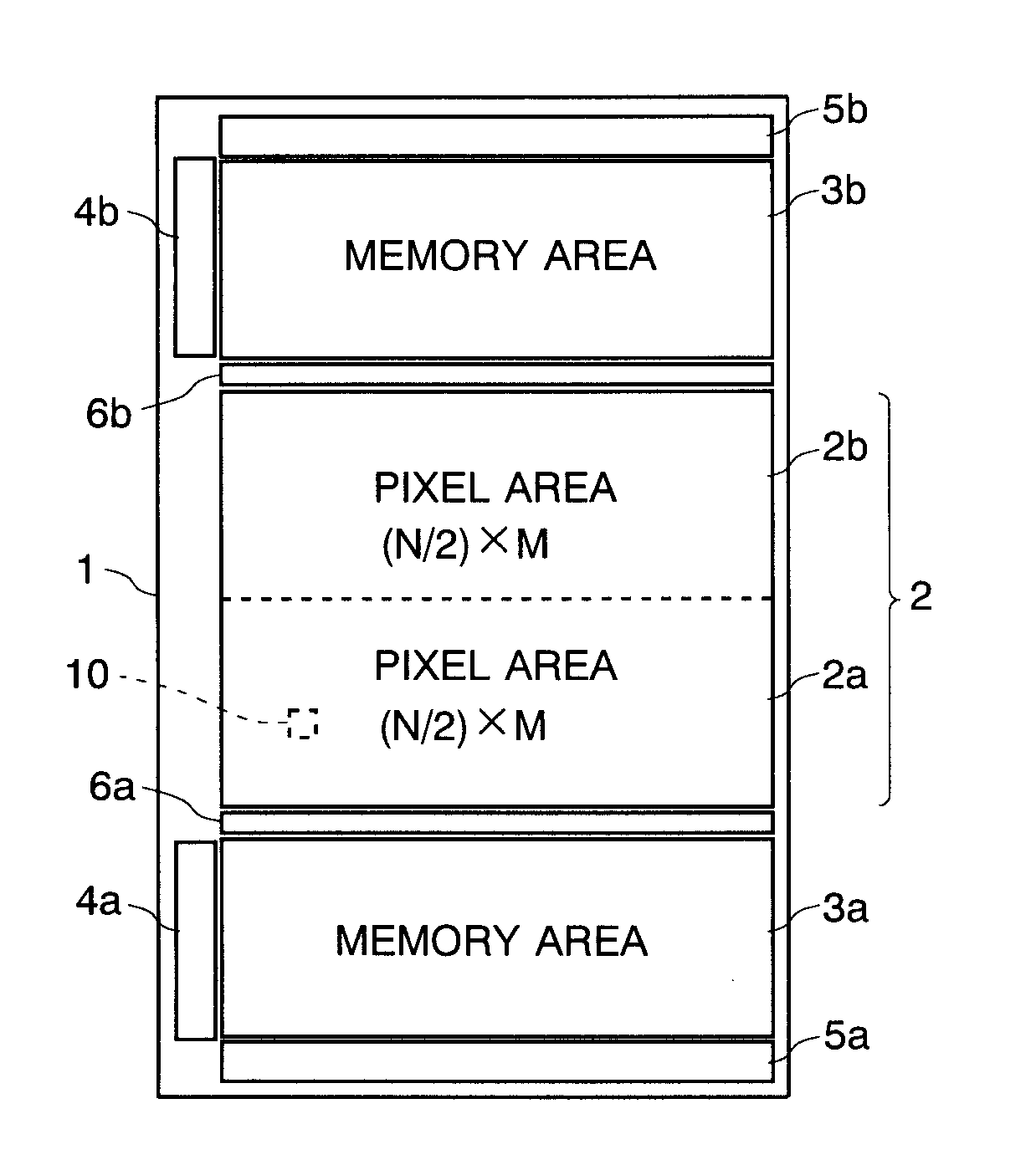
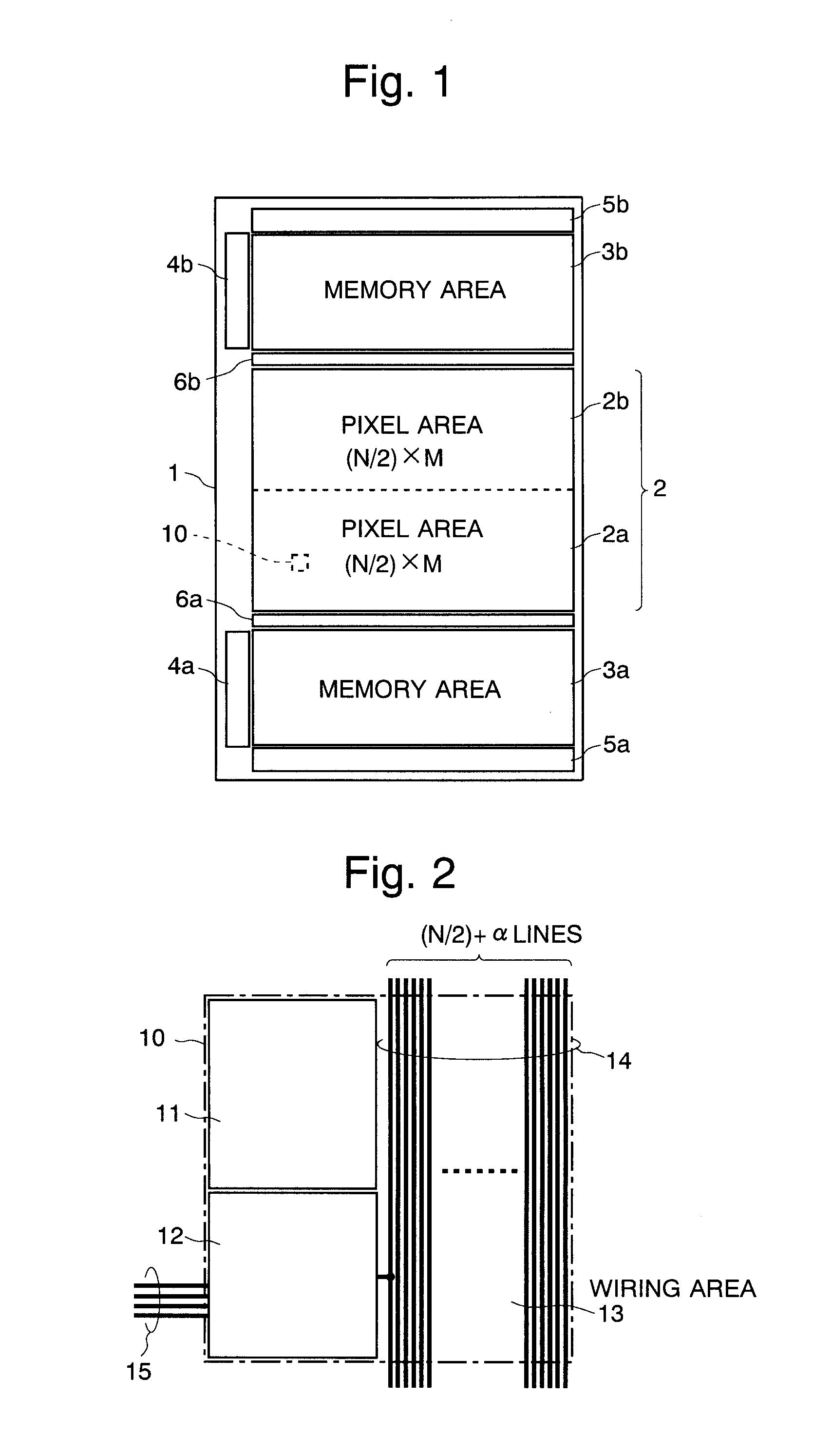
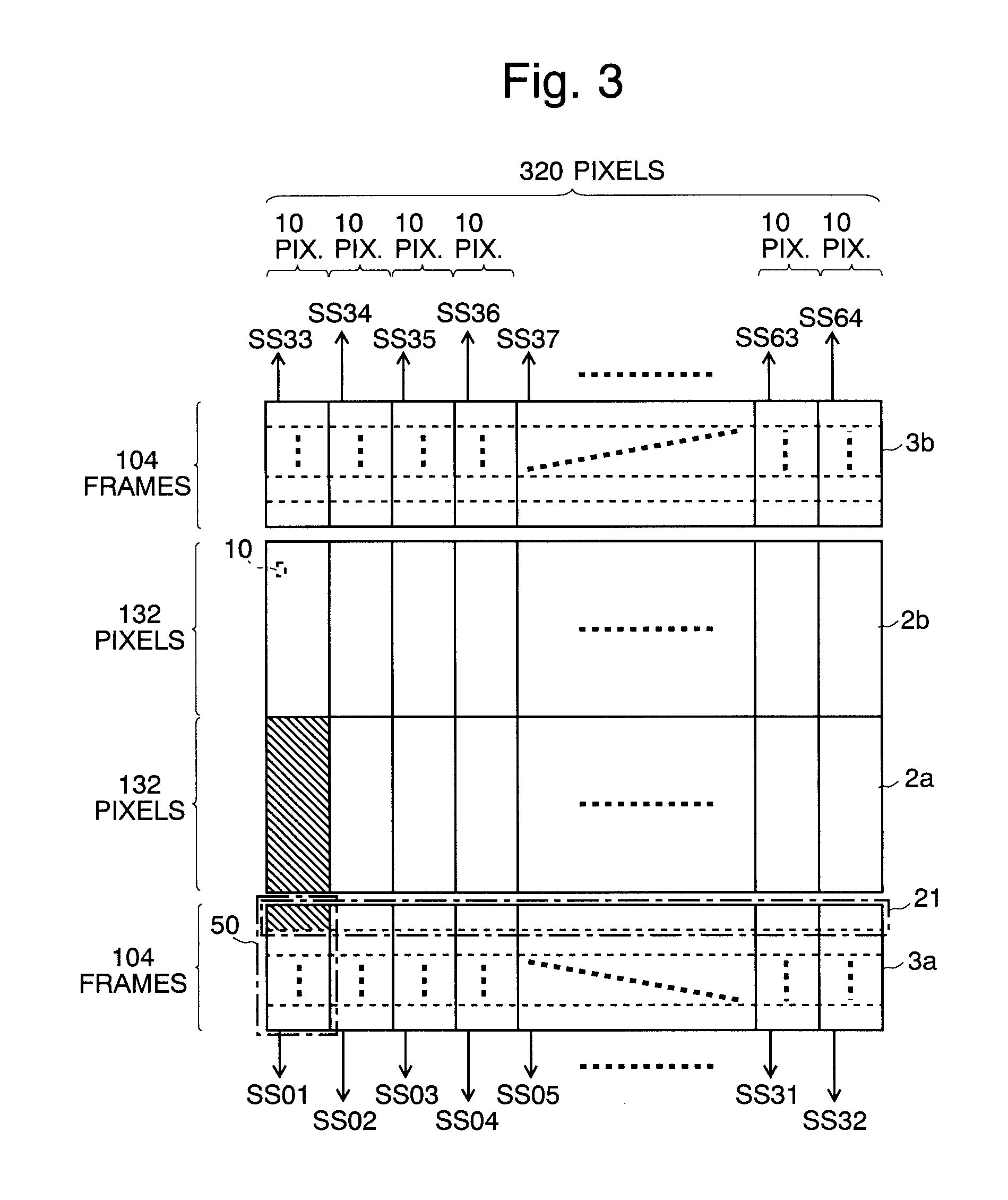
[0115]An overall configuration and structure of the solid-state image sensor according to the present embodiment is initially described. FIG. 1 is a schematic plan view showing the layout on a semiconductor chip of the solid-state image sensor of the present embodiment, FIG. 3 is a plan view showing a schematic configuration of the pixel area and memory area in the solid-state image sensor of the present embodiment, and FIG. 4 is a block diagram of the main portion corresponding to approximately one-half of the semiconductor chip of the solid-state image sensor of the present embodiment.

[0116]As shown in FIG. 1, in the present solid-state image sensor, the pixel area 2 (2a and 2b) for receiving light and producing signals for each pixel and the memory areas 3a and 3b for holding the signals for a predetermined number of frames ...


PUM


Abstract

An independent pixel output line (14) is provided for each of two-dimensionally arranged pixels (10) within a pixel area (2a). A plurality of memory sections are connected to each pixel output line (14). In a continuous reading mode, photocharge storage is simultaneously performed at all the pixels, and signals are collectively transferred from the pixels (10) through the pixel output lines (14) to the memory sections, after which the signals held in the memory sections are sequentially read and outputted. In a burst reading mode, the operations of simultaneously storing photocharges at all the pixels and collectively transferring signals from each pixel (10) through the pixel output line (14) to the memory sections are sequentially performed for each of the memory sections to hold signals corresponding to a plurality of frames. When a imaging halt command is given, the holding of new signals is halted, and a plurality of frames of image signals held in the memory sections at that point in time are sequentially read and outputted. Thus, both an ultrahigh-speed imaging operation with a limitation on the number of frames and an imaging mode that is rather slow but has no limitation on the number of frames can be performed.

Description

TECHNICAL FIELD[0001]The present invention relates to a solid-state image sensor and a drive method for this sensor. More specifically, it relates to a solid-state image sensor capable of high-speed operations suitable for taking images of high-speed phenomena such as destructions, explosions and combustions, and a drive method for such a sensor.BACKGROUND ART[0002]High-speed imaging devices (high-speed video cameras) for taking consecutive images of high-speed phenomena such as explosions, destructions, combustions, collisions and discharges for only a short period of time have been conventionally developed (for example, refer to Non-Patent Document 1 and other documents). Such high-speed imaging devices need to perform an ultrahigh-speed imaging operation that exceeds a level of approximately one million frames per second. Accordingly, they use solid-state image sensors capable of high-speed operations, which have special structures different from those of the imaging devices conv...

Claims


Application Information

Patent Timeline
IPC IPC(8): H04N5/335H04N5/355H04N5/357H04N5/374H04N5/3745H04N5/378
CPCH04N5/35572H04N5/3575H04N5/3559H04N5/37452H04N5/378H04N5/3742H04N25/587H04N25/59H04N25/616H04N25/767H04N25/771H04N25/75
Inventor SUGAWA, SHIGETOSHIKONDO, YASUSHITOMINAGA, HIDEKI
Owner TOHOKU UNIV
Why Eureka
Try Eureka