Solid-state imaging device, driving method thereof, and imaging apparatus

a technology of solid-state imaging and driving method, which is applied in the direction of exposure control, instruments, television systems, etc., can solve the problem of difficulty in obtaining a wide dynamic range appropriately

Inactive Publication Date: 2010-08-12
SONY SEMICON SOLUTIONS CORP
View PDF5 Cites 18 Cited by
  • Summary
  • Abstract
  • Description
  • Claims
  • Application Information

AI Technical Summary

Benefits of technology

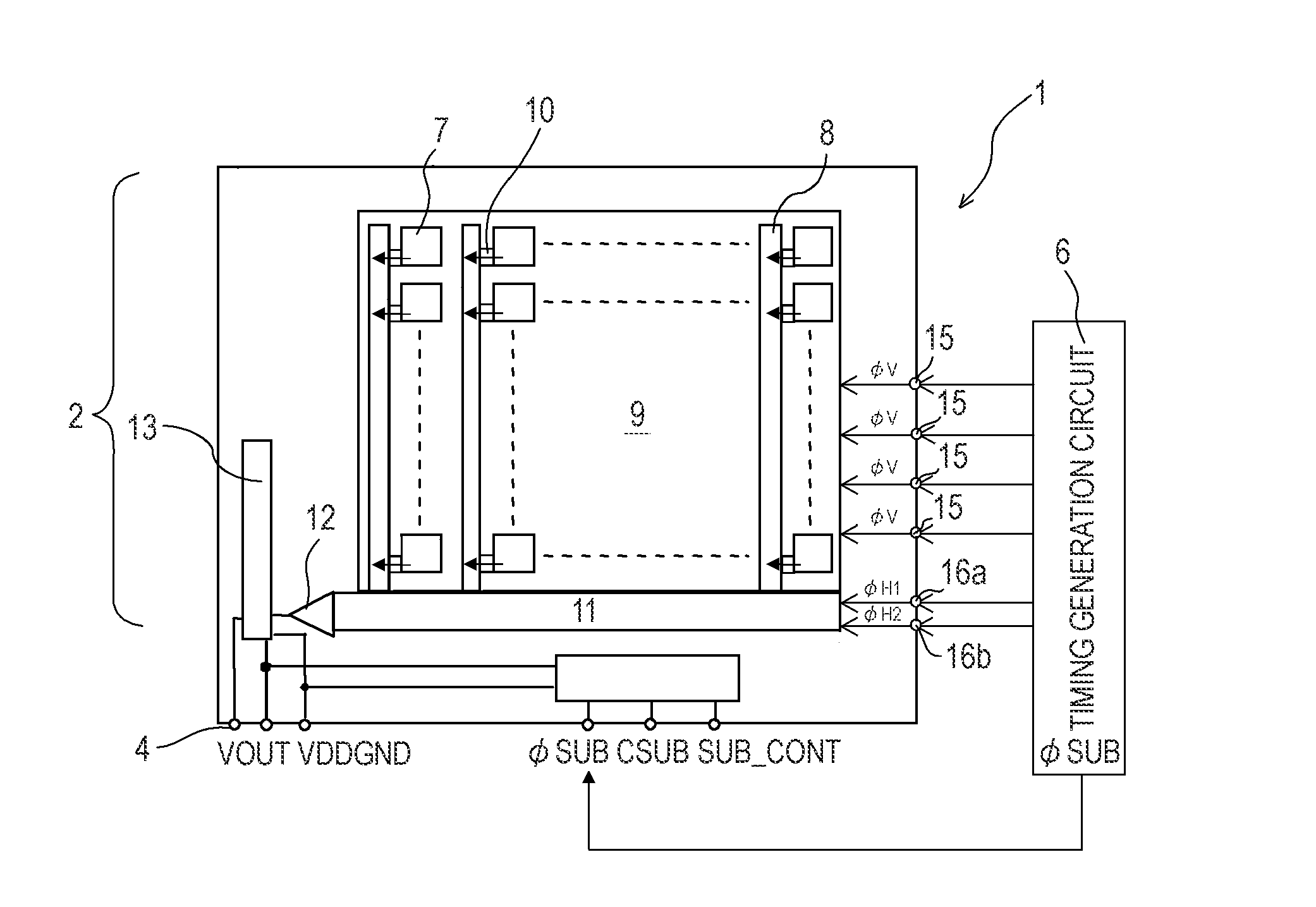
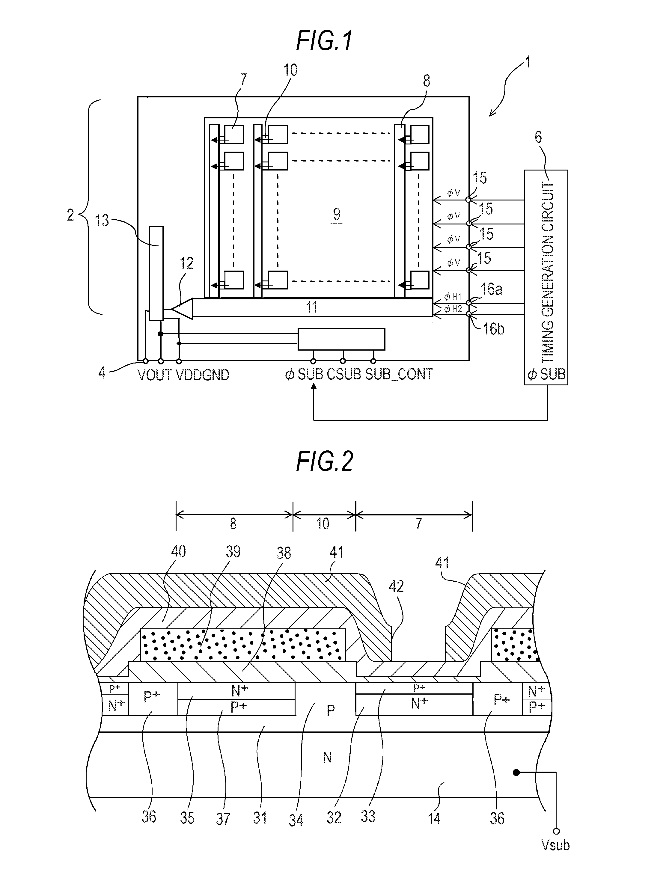
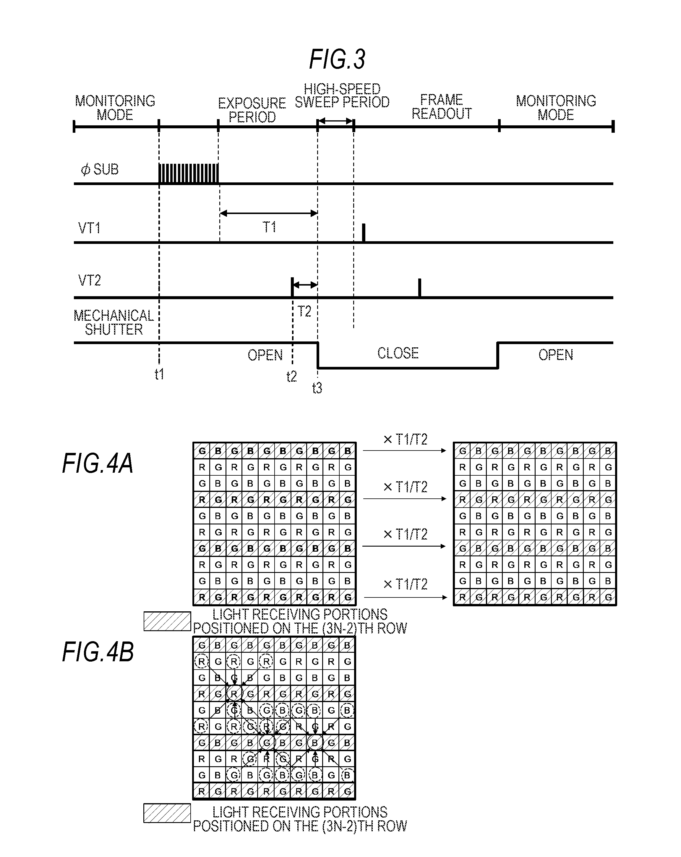
[0036]According to the solid-state imaging device, the driving method thereof, and the imaging apparatus of the above-mentioned embodiments of the present invention, it is possible to obtain image signals with different exposure periods using the same readout sequence.

Problems solved by technology

It is therefore difficult to obtain a wide dynamic range appropriately.

Method used


Image

  • Solid-state imaging device, driving method thereof, and imaging apparatus
  • Solid-state imaging device, driving method thereof, and imaging apparatus
  • Solid-state imaging device, driving method thereof, and imaging apparatus

Examples


second embodiment

2. Second Embodiment

[0102]In the first embodiment described above, the case of obtaining two image signals with different exposure periods has been described as an example. However, the number of image signals being combined is not necessarily two, and three or more image signals with different exposure periods may be combined together. In the case of obtaining three or more image signals with different exposure periods, the configuration of the solid-state imaging device is the same as that used in the first embodiment described above.

Operation of Solid-State Imaging Device

[0103]Hereinafter, the operation of the solid-state imaging device of the case of obtaining three image signals with different exposure periods will be described. That is, another example of a driving method of the solid-state imaging device according to the embodiment of the present invention will be described.

Acquisition of Voltage Signal with Different Exposure Periods

[0104]In the case of obtaining three image...

third embodiment

3. Third Embodiment

Configuration of Wide D Camera

[0141]FIG. 8 is a block diagram illustrating a general configuration of a wide dynamic range camera (hereinafter referred to as a “wide D camera”) which is an example of an imaging apparatus according to an embodiment of the present invention.

[0142]The wide D camera illustrated in FIG. 8 includes an optical component 130, an image sensor 131, a pre-processing portion 132, a signal processing portion 133, an output portion 134, a TG 135, an EVR 136, a microcomputer 137, an optical component control circuit 138, and a recording medium 139.

[0143]The optical component 130 is a lens or an optical filter that removes unnecessary wavelength components, and may be an ND (neutral density) filter, for example, which is a light-intensity adjustment filter. Light which has been incident from a subject and has passed through the optical component 130 is captured by the image sensor 131 and is then converted to electrical signals. Moreover, the opt...


PUM


Abstract

A solid-state imaging device includes: light receiving portions that accumulate signal charges corresponding to incident light; charge transfer portions that are formed to be adjacent to the light receiving portions so as to transfer the signal charges readout from the light receiving portions; readout electrodes to which a readout voltage for reading out the signal charges accumulated in the light receiving portions to the charge transfer portions is applied; and a controller that is configured to be able to apply the readout voltage to the readout electrodes corresponding to first predetermined light receiving portions which are part of the light receiving portions in an exposure period when the signal charges are accumulated in the light receiving portions.

Description

BACKGROUND OF THE INVENTION[0001]1. Field of the Invention[0002]The present invention relates to a solid-state imaging device, a driving method thereof, and an imaging apparatus. More particularly, the present invention relates to a solid-state imaging device capable of achieving a wide dynamic range, a driving method thereof, and an imaging apparatus using the solid-state imaging device capable of achieving a wide dynamic range.[0003]2. Description of the Related Art[0004]Recently, video cameras, still digital cameras, and other apparatuses using solid-state image sensors such as CCDs (charge coupled devices) have become popular.[0005]FIG. 12 is a diagram illustrating a still-image exposure sequence of the related art. According to a driving method of a solid-state imaging device according to the related art, the still-image exposure sequence includes a high-speed imaging period (monitoring mode), an exposure period, a high-speed sweep period, and a frame readout period. The still-...

Claims


Application Information

Patent Timeline
Patent Type & Authority Applications(United States)
IPC IPC(8): H04N5/335H04N5/235H04N5/353H04N5/355H04N5/3728H04N5/376
CPCH04N5/3535H04N5/3728H04N5/35554H04N25/533H04N25/583H04N25/73
Inventor HATABU, KAZUAKI
Owner SONY SEMICON SOLUTIONS CORP
Why Eureka
Try Eureka