Magnetic field sensor device for direct magnetic field imaging and method of fabrication thereof

a magnetic field and sensor device technology, applied in the direction of magnetic field measurement using superconductive devices, scanning probe techniques, instruments, etc., can solve the problem of poor spatial resolution (of several microns)

Active Publication Date: 2010-08-19
YEDA RES & DEV CO LTD
View PDF5 Cites 23 Cited by
  • Summary
  • Abstract
  • Description
  • Claims
  • Application Information

AI Technical Summary

Problems solved by technology

Scanning SQUID microscopy [3] has the highest field sensitivity (...

Method used


Image

  • Magnetic field sensor device for direct magnetic field imaging and method of fabrication thereof
  • Magnetic field sensor device for direct magnetic field imaging and method of fabrication thereof
  • Magnetic field sensor device for direct magnetic field imaging and method of fabrication thereof

Examples


Embodiment Construction

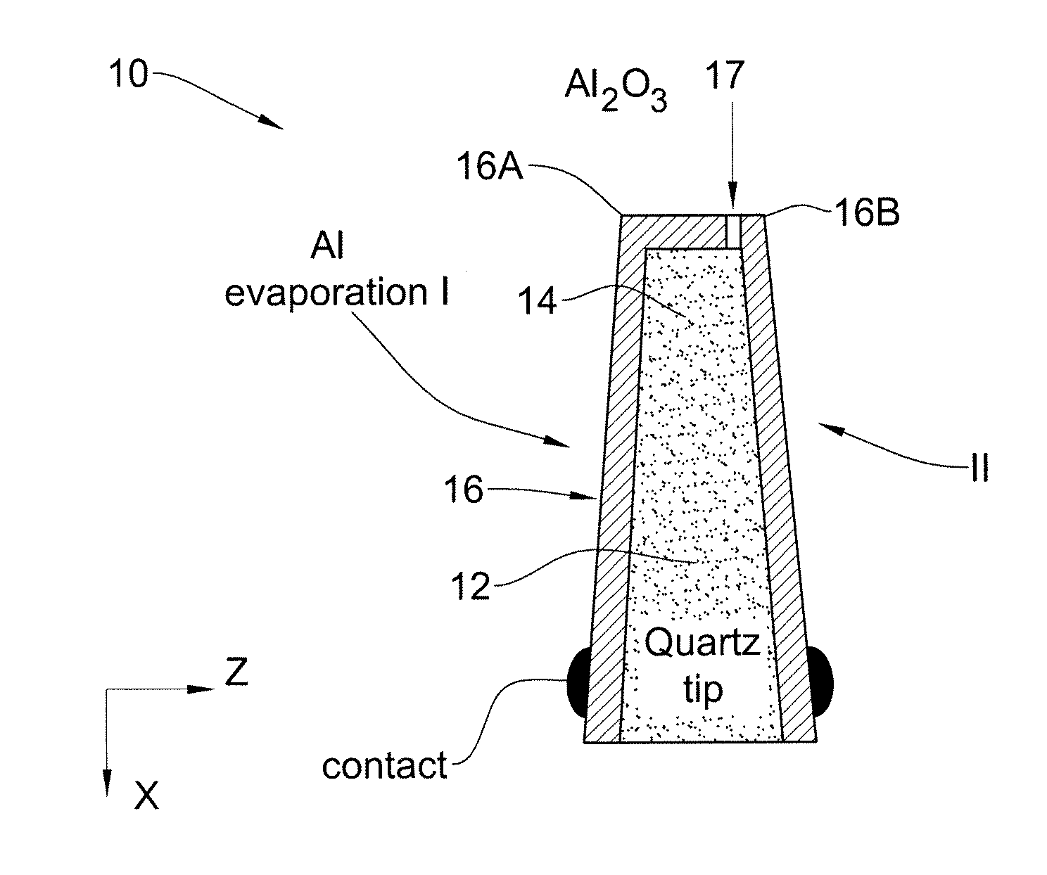
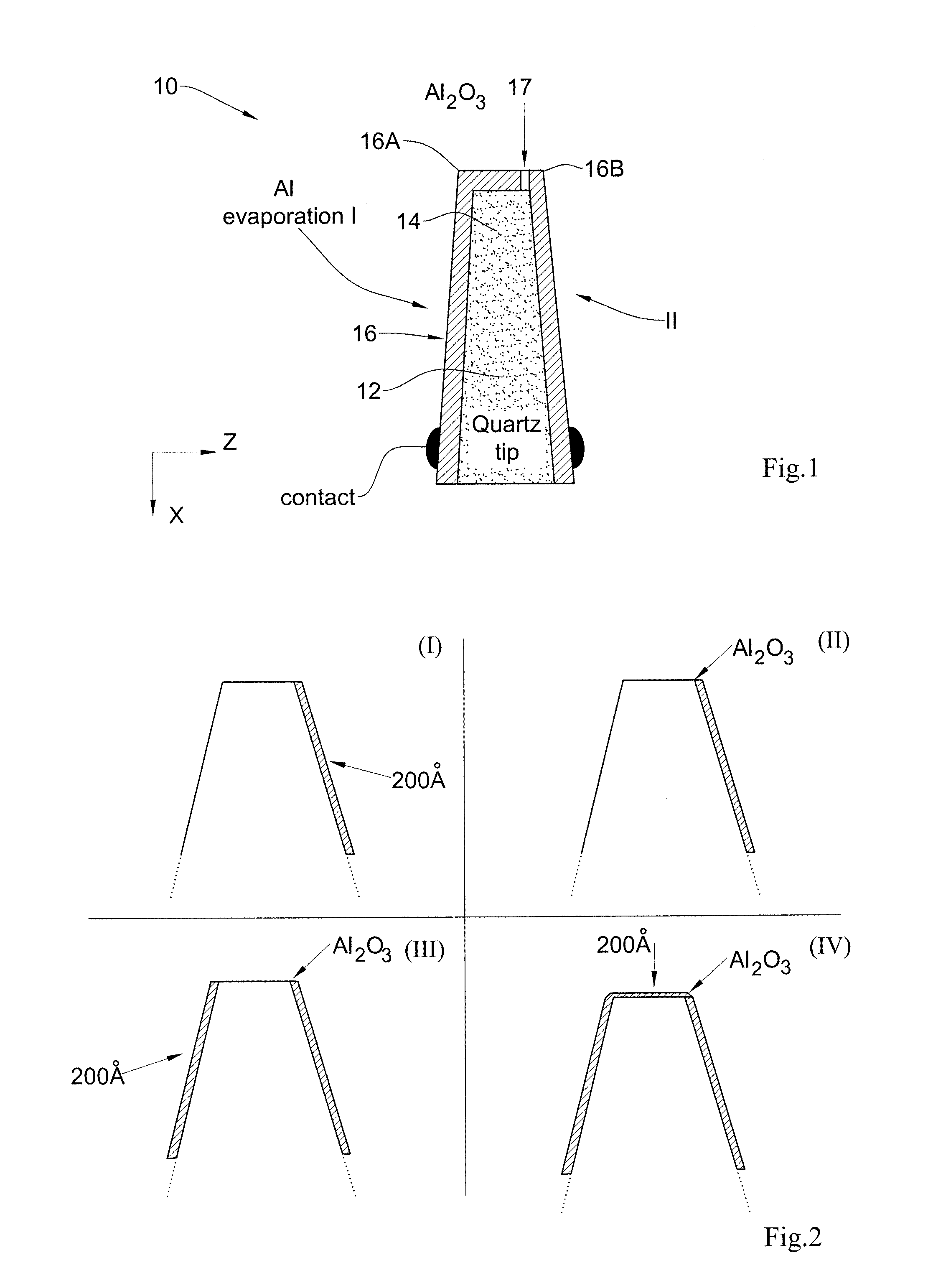
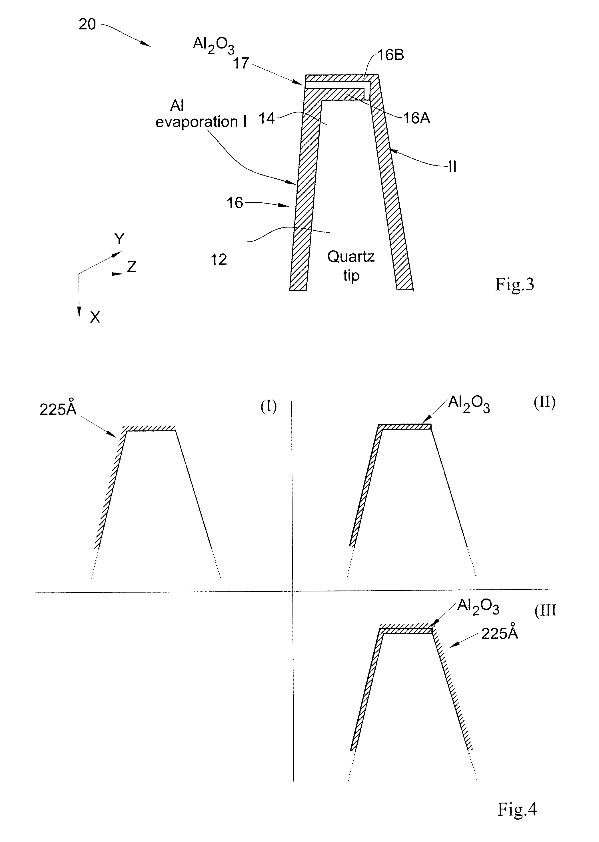
[0065]Referring to FIG. 1, there is illustrated an example of a magnetic field sensor device, generally designated 10. The device is configured as a Josephson junction based sensor having a single tunnel junction, with vertical field sensitivity (in which the sensitivity of the sensor is parallel to the rod, represented in FIG. 1 to be in the X direction). The device 10 includes a conically shaped core 12 having an apex portion 14, thus defining a tip-like portion; and an electrodes arrangement defined by two separate (spaced-apart) portions 16A and 16B of a superconducting film 16 which is coated on at least a part of the conical core 12 including its apex 14. Within the apex 14, the film coating 16 is broken and is separated by an insulator 17 thus defining a tunneling region between the electrodes 16A and 16B. Hence, a single Josephson junction (JJ) with vertical field sensitivity is created, in which the junction is parallel to the magnetic field in the X direction.

[0066]The dev...


PUM

PropertyMeasurementUnit
Pressureaaaaaaaaaa
Diameteraaaaaaaaaa
Magnetic fieldaaaaaaaaaa

Abstract

The present invention discloses a novel magnetic sensor device performing direct magnetic field imaging, comprising a probe having a conical tip portion which is configured as a sensor having two superconductors separated by a thin non-superconducting layer (such as a Josephson junction based sensor), where the non-superconducting layer is located at the apex portion of said conical tip, thereby defining electron tunneling region(s) at said apex portion. The technique of the present invention enables the sensor device to be very small and to be brought very close to the sample surface.

Description

FIELD OF THE INVENTION[0001]This invention relates to local magnetic field sensor devices for direct magnetic field imaging and method of fabrication thereof.REFERENCES[0002]The following references are considered to be pertinent for the purpose of understanding the background of the present invention:[0003]1. K. Harada, T. Matsuda, J. Bonevich, M. Igarashi, S. Kondo, G. Pozzi, U. Kawabe, and A. Tonomura, Nature 360, 51 (1992).[0004]2. H. J. Hug, A. Moser, I. Parashikov, B. Stiefel, O. Fritz, H.-J. Güntherodt, and H. Thomas, Physica C 235-240, 2695 (1994).[0005]3. J. R. Kirtley, C. C. Tsuei, J. Z. Sun, C. C. Chi, Lock See Yu-Jahnes, A. Gupta, M. Rupp, and M. B. Ketchen, Nature 373, 225 (1995).[0006]4. B. L. T. Plourde and D. 3. V. Harlingen, Review of Scientific Instruments 70, 4344 (1999).[0007]5. Likharev, K. K. Superconducting weak links. Rev. Mod. Phys. 51, 101, (1979).[0008]6. A. Yacoby, H. F. Hess, T. A. Fulton, L. N. Pfeiffer and K. W. West, Solid State Communications 111, 1 ...

Claims


Application Information

Patent Timeline
IPC IPC(8): G01R33/035H01B19/00
CPCG01R33/0385G01R33/0354B82Y35/00B82Y25/00Y10T29/49227G01Q60/56H10N60/0912
Inventor FINKLER, AMITMARTIN, JENSMYASOEDOV, YURISEGEV, YEHONATHANYACOBY, AMIRZELDOV, ELI
Owner YEDA RES & DEV CO LTD
Why Eureka
Try Eureka