Display Device and Method for Fabricating the same

a technology for display devices and manufacturing methods, applied in the manufacture of electrode systems, electric discharge tubes/lamps, instruments, etc., can solve problems such as permeability into display devices, and achieve the effect of high packaging reliability

Active Publication Date: 2010-08-19
E INK HLDG INC
View PDF13 Cites 36 Cited by
  • Summary
  • Abstract
  • Description
  • Claims
  • Application Information

AI Technical Summary

Benefits of technology

[0006]The invention is directed to a displ

Problems solved by technology

However, the sealant 14 may be slit as the display device 10 is bent several times. Thus, the air or mist from outside may permeate into the display device 10 and damage it.
Therefore, it is one of the important is

Method used


Image

  • Display Device and Method for Fabricating the same
  • Display Device and Method for Fabricating the same
  • Display Device and Method for Fabricating the same

Examples


Embodiment Construction

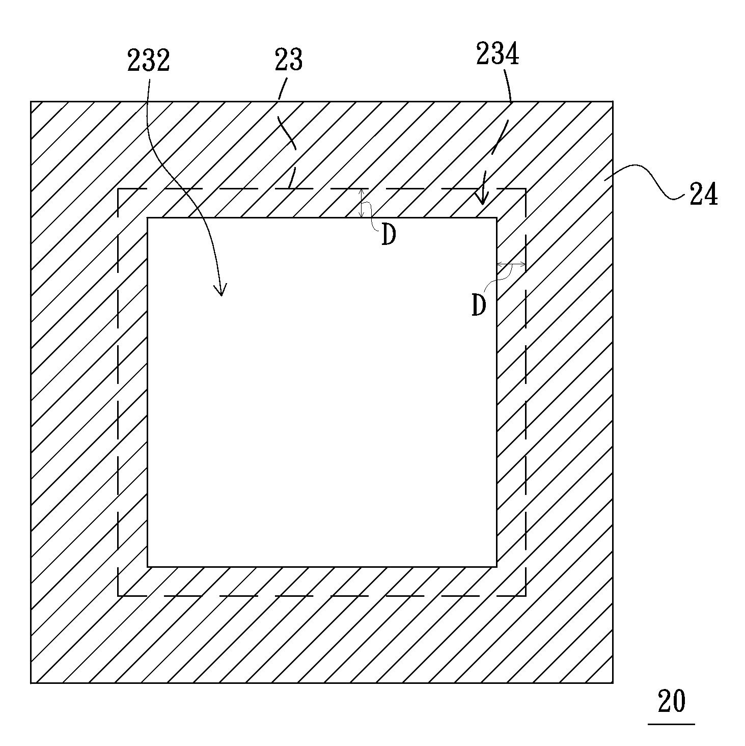
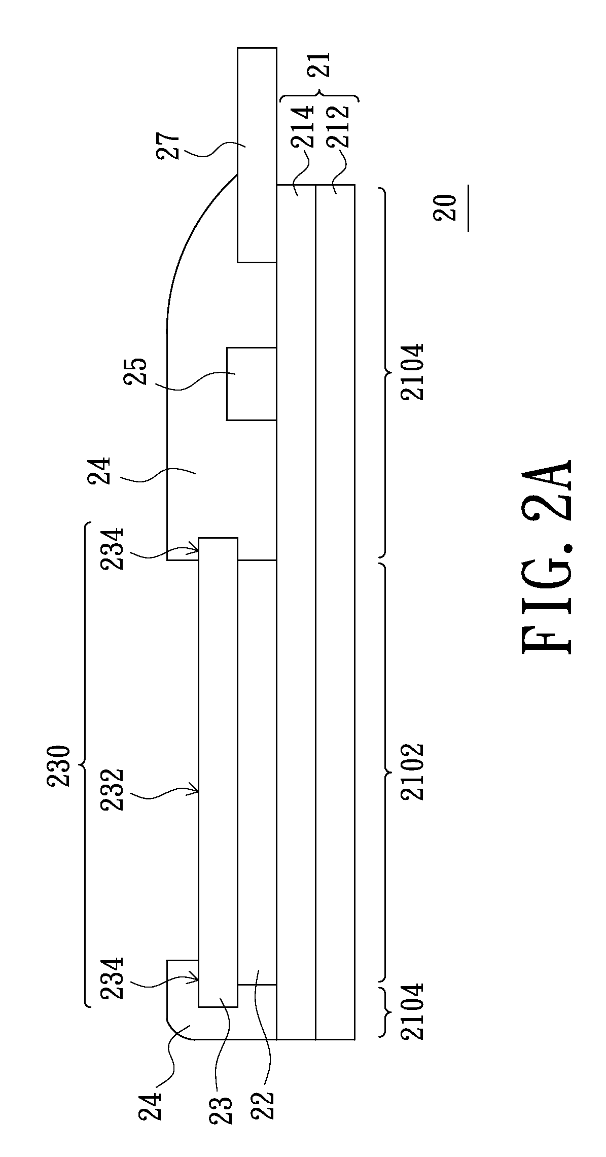
[0017]FIG. 2A is a schematic cross-sectional view of the display device according to an embodiment of the invention. Referring to FIG. 2A, the display device 20 comprises an array substrate 21, a display medium layer 22, a transparent layer 23 and a sealant 24. The array substrate 21 has a first region 2102 and a second region 2104 surrounding the first region 2102. In detail, the array substrate 21 comprises a substrate 212 and a switch elements array 214 disposed thereon. The substrate 212 may be a flexible substrate. That is, the display device 20 may be a flexible display device. The switch elements array 214 may be an active elements array or a passive elements array. In this embodiment, the switch elements array 214 may be a thin film transistors array.

[0018]The display medium layer 22 is disposed on the array substrate 21 and located in the first region 2102. The transparent layer 23 is disposed on the display medium layer 22 and has an upper surface 230 with a display region...


PUM


Abstract

A display device includes an array substrate, a display medium layer, a transparent layer and a sealant. The array substrate has a first region and a second region surrounding the first region. The display medium layer is disposed on the array substrate and located in the first region. The transparent layer with an upper surface is disposed on the display medium layer. The upper surface has a display region and a predetermined sealing region surrounding the display region. The sealant is formed on the array substrate and located in the second region. Also, the sealant surrounds the transparent layer and the display medium layer and covers the predetermined sealing region of the transparent layer. In addition, a method for fabricating the display device is also provided. Since the sealant surrounds the transparent layer and the display medium layer and covers the predetermined sealing region of the transparent layer, the packaging performance of the above display device may be improved.

Description

BACKGROUND[0001]This application claims priority to a Taiwan application No. 098105339 filed Feb. 19, 2009.FIELD OF THE INVENTION[0002]The invention relates to a display device and method for fabricating the same, and more particular to a display device with high packaging reliability and method for fabricating the same.DESCRIPTION OF THE RELATED ART[0003]With progress of science and technology, display devices are used in any electric products popularly. Moreover, since the development trend of the portable electrical product is to achieve light weight and thin thickness, the flexible display device are researched.[0004]FIG. 1 is a schematic cross-sectional view of the conventional flexible display device. Referring to FIG. 1, the display device 10 comprises a flexible array substrate 11, a display medium layer 12, a transparent layer 13, a sealant 14, a driver IC 15 and a flexible circuit board 16. The flexible array substrate 11 comprises a substrate 112 and a thin film transisto...

Claims


Application Information

Patent Timeline
IPC IPC(8): G02F1/1339H01J9/20H01L27/12
CPCG02F1/13452H05K1/189G02F2001/133311H01L2251/5338H01L51/5237G02F1/133305H05K3/284G02F1/133311H10K2102/311H10K59/8722H10K50/8426
Inventor TSAI, YUAN-CHIHSHINN, TED-HONGWANG, YI-CHING
Owner E INK HLDG INC
Why Eureka
Try Eureka