Surface mounted package with die bottom spaced from support board

a technology of support board and die bottom, which is applied in the direction of semiconductor devices, semiconductor/solid-state device details, electrical apparatus, etc., can solve the problems of die-underfill bonding, underfill-substrate bonding, solder bump attachment and passivation layer, etc., and reduce the reliability of the package

Inactive Publication Date: 2005-08-16
INFINEON TECH AMERICAS CORP
View PDF42 Cites 27 Cited by
  • Summary
  • Abstract
  • Description
  • Claims
  • Application Information

AI Technical Summary

Benefits of technology

[0007]In order to reduce substrate failure, for example, caused by thermal cycling a semiconductor device package is disclosed that comprises a semiconductor device die having a first surface substantially parallel to a second surface, and the first surface and second surface each have a solderable planar metal electrode. Further, a metal clip is disclosed that has a flat web portion comprising a first and second surface, wherein the second surface is electrically connected with the first surface of the semiconductor device die.

Problems solved by technology

Generally, thermal cycling causes frequent and repeated stress which in layered structures leads to cracks due to, for example, fatigue.
In semiconductor device packages, temperature cycling causes failures in die-underfill bonding, underfill-substrate bonding, solder bump attachment and passivation layers among other areas.
This reduces the reliability of the package.

Method used


Image

  • Surface mounted package with die bottom spaced from support board
  • Surface mounted package with die bottom spaced from support board
  • Surface mounted package with die bottom spaced from support board

Examples


Embodiment Construction

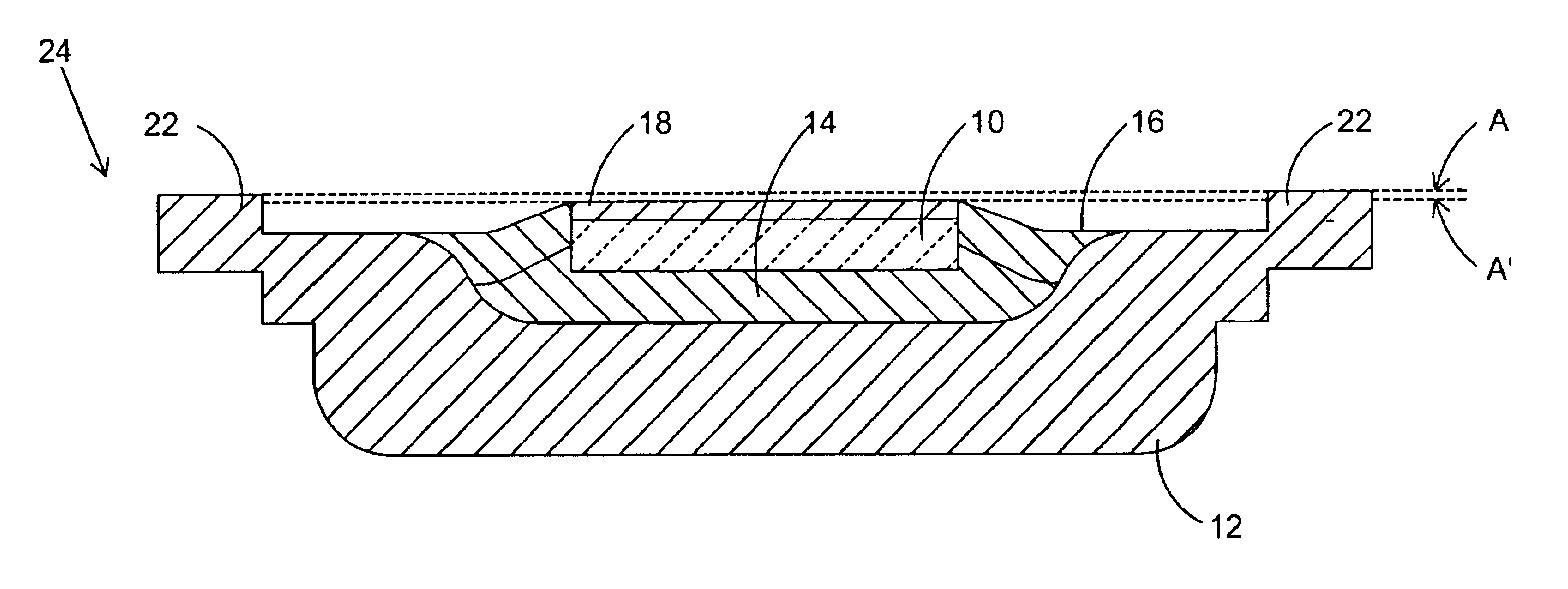
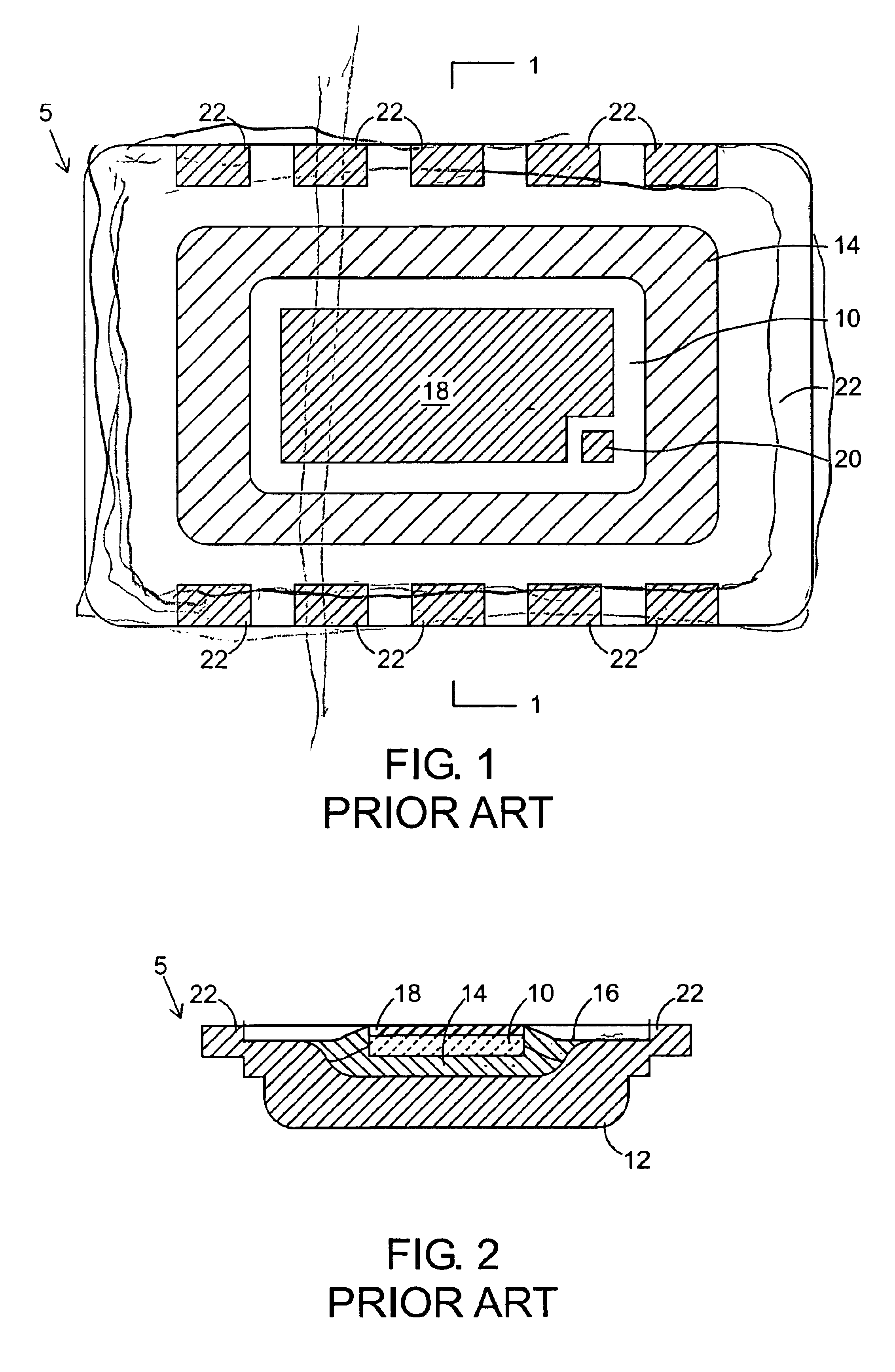
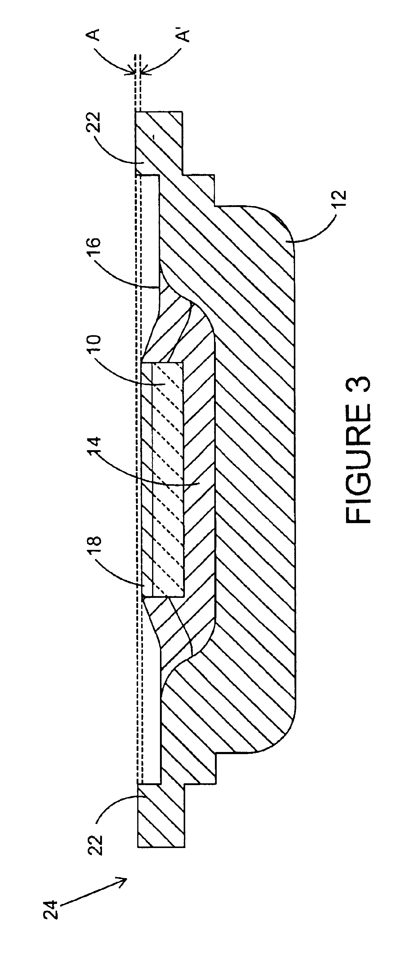
[0015]Referring now to FIG. 3, in accordance with the present invention, semiconductor package 24 includes MOSFET 10 that is set back deeper into the interior of can 12 than in prior art packages as shown in FIG. 1 and FIG. 2. Therefore, source contact 18 and gate contact 20 (not shown in FIG. 3) of MOSFET 10 are no longer flush with projections 22 of can 12. This arrangement is illustrated in FIG. 3 by the gap between broken lines A, A′. It has been found that when MOSFET 10 is set deeper within can 12 such that source 18 is offset from the plane of the circuit board (as represented by broken line A) by about 0.001-0.005 inches failure due to thermal cycling of the part when soldered down or affixed by an epoxy to a substrate is reduced.

[0016]In other words, a semiconductor package according to the present invention includes a metal can which receives in its interior space a MOSFET or other similar semiconductor type device die. The MOSFET so received is inwardly recessed in the ca...


PUM


Abstract

A semiconductor package according to the present invention includes a metal can which receives in its interior space a MOSFET. The MOSFET so received is oriented such that its drain electrode is facing the bottom of the can and is electrically connected to the same by a layer of conductive epoxy or a solder or the like. The edges of the MOSFET so placed are spaced from the walls of the can. The space between the edges of the MOSFET and the walls of the can is filled with an insulating layer. A surface of the MOSFET is sub-flush below the plane of a substrate by 0.001-0.005 inches to reduce temperature cycling failures.

Description

CROSS-REFERENCE TO RELATED APPLICATION[0001]This application is based on and claims priority to U.S. Provisional Application No. 60 / 342,333, filed on Dec. 21, 2001, by Martin Standing and Andrew N. Sawle, entitled “SURFACE MOUNTED PACKAGE WITH DIE BOTTOM SPACED FROM SUPPORT BOARD,” and is a continuation-in-part application of U.S. patent application Ser. No. 09 / 819,774, filed on Mar. 28, 2001 now U.S. Pat. No. 6,624,522, by Martin Standing and Hazel Deborah Schofield, entitled “CHIP SCALE SURFACE MOUNTED DEVICE AND PROCESS OF MANUFACTURE,” the subject matter and disclosure of both applications being incorporated by reference herein.FIELD OF THE INVENTION[0002]The present invention relates to a semiconductor package and more particularly to a semiconductor package for housing a power semiconductor die having a structure which reduces temperature cycling failures.BACKGROUND OF THE INVENTION[0003]Generally, thermal cycling causes frequent and repeated stress which in layered structures...

Claims


Application Information

Patent Timeline
Patent Type & Authority Patents(United States)
IPC IPC(8): H01L23/31H01L23/28H01L23/492H01L23/48H01L23/04H01L23/047H01L23/13H01L23/34
CPCH01L23/047H01L23/13H01L23/3114H01L23/492H01L24/34H01L2924/1305H01L2924/1301H01L2924/1306H01L2224/37147H01L2224/73253H01L2224/32245H01L2924/01074H01L2924/01047H01L2924/01006H01L2224/73153H01L2924/01029H01L2924/01033H01L2924/01057H01L2924/01078H01L2924/01082H01L2924/13055H01L2924/13091H01L2924/00H01L24/37H01L2224/06181H01L2224/83801H01L2224/8385H01L2224/0603H01L2924/00014
Inventor STANDING, MARTINSAWLE, ANDREW NEIL
Owner INFINEON TECH AMERICAS CORP
Why Eureka
Try Eureka