Semiconductor device

a technology of semiconductor devices and external terminals, which is applied in the direction of semiconductor devices, semiconductor/solid-state device details, electrical apparatus, etc., can solve the problems of brittle fracture, hardness, elasticity, etc., of low-k materials such as hardness, elasticity, etc., and achieve the effects of enhancing packaging reliability, and increasing the size and pitch of the external terminals

Active Publication Date: 2006-01-19
RENESAS ELECTRONICS CORP
View PDF1 Cites 25 Cited by
  • Summary
  • Abstract
  • Description
  • Claims
  • Application Information

AI Technical Summary

Benefits of technology

[0022] An object of the present invention is to provide a highly reliable semiconductor device that is provided with a huge wiring structure portion on a minute wiring structure portion, relieving stress occurring in the minute wiring structure portion, has large driving current and operates at high frequency.
[0024] In the present invention, the first huge wiring structure portion in which the second wiring layer has a thickness of twice or more of the thickness of the first wiring layer and the second insulating layer are alternately laminated is provided on the minute wiring structure portion which is provided on the semiconductor substrate and in which the first wiring layer and the first insulating layer are alternately laminated, and further the second huge wiring structure portion in which the third wiring layer has a thickness of twice or more of the thickness of the first wiring layer and the third insulating layer has the elastic modulus at 25° C. which is not more than that of the second insulating layer are alternately laminated is provided on the first huge wiring structure portion. Therefore, the stress occurring in the semiconductor device after the semiconductor device is mounted on the mount board can be effectively relieved in the first huge wiring structure portion and the second huge wiring structure portion, and the stress imposed on the minute wiring structure portion can be reduced.
[0031] Still furthermore, each of the first wiring layer, the second wiring layer and the third wiring layer has a plurality of power source system wires, and one wire of the plural power source system wires of the second wiring layer or the third wiring layer may be electrically connected to two or more power source system wires of the plural power source system wires of the first wiring layer. In this case, one wire of the plural power source system wires of the third wiring layer may be electrically connected to two or more power source system wires of the plural power source system wires of the second wiring layer. As described above, in the second wiring layer and / or the third wiring layer having a larger permissible current amount than the first wiring layer, two or more power source system wires using the same voltage are integrated into one wire, whereby the number of external terminals provided on the second huge wiring structure portion with respect to the number of connection terminals on the minute wiring structure portion can be reduced. Accordingly, the size and pitch of the external terminals can be increased and the packaging reliability can be enhanced.
[0032] Still furthermore, each of the first wiring layer, the second wiring layer and the third wiring layer may have plural ground system wires, and one wire of the plural ground system wires of the second wiring layer or the third wiring layer may be electrically connected to two or more ground system wires of the plural ground system wires of the first wiring layer. In this case, one wire of the plural ground system wires of the third wiring layer may be electrically connected to two or more ground system wires of the plural ground system wires of the second wiring layer. As described above, in the second wiring layer and / or the third wiring layer having a larger permissible current amount than the first wiring layer, two or more ground system wires using the same voltage are integrated into one wire, whereby the number of external terminals provided on the second huge wiring structure portion with respect to the number of connection terminals on the minute wiring structure portion can be reduced. Therefore, the size and pitch of the external terminals can be increased and the packaging reliability can be enhanced.
[0033] Each of the first wiring layer, the second wiring layer and the third wiring layer may have plural power source system wires and plural ground system wires, one wire of the plural power source system wires of the third wiring layer or the second wiring layer may be electrically connected to two or more power source system wires of the plural power source system wires of the first wiring layer, and one wire of the plural ground system wires of the third wiring layer and the second wiring layer may be electrically connected to two or more ground system wires of the plural ground system wires of the first wiring layer. In this case, one wire of the plural power source system wires of the third wiring layer may be electrically connected to two or more power source system wires of the plural power source system wires of the second wiring layer, and one wire of the plural ground system wires of the third wiring layer may be electrically connected to two or more ground system wires of the plural ground system wires of the second wiring layer. As described above, in the second wiring layer and / or the third wiring layer having a permissible current amount larger than the first wiring layer, two or more power system wires using the same voltage can be integrated into one wire, and also two or more ground system wires using the same voltage are integrated into one wire, whereby the number of external terminals provided on the second huge wiring structure portion with respect to the number of connection terminals on the minute wiring structure portion can be effectively reduced, so that the size and pitch of the external terminals can be increased and thus the packaging reliability can be enhanced.
[0034] According to the present invention, the first huge wiring structure portion in which the second wiring layer(s) having a thickness of twice or more of the thickness of the first wiring layer and the second insulating layer(s) are alternately laminated is provided on the minute wiring structure portion in which the first wiring layer(s) and the first insulating layer(s) are alternately laminated, and the second huge wiring structure portion in which the third wiring layer(s) having a thickness of twice or more of the thickness of the first wiring layer(s) and the third insulating layer(s) having the elastic modulus at 25° C. which is not more than that of the second insulating layer are alternately laminated is provided on the first huge wiring structure portion, whereby the stress occurring after the semiconductor device is mounted on the mount board can be effectively relieved by the first huge wiring structure portion and the second huge wiring structure portion, and thus the stress imposed on the minute wiring structure portion can be reduced. Furthermore, the plural power source system wires and / or the ground system wires are integrated, whereby the number of external terminals can be reduced and the number of external terminals and / or the pitch can be increased. As a result, there can be provided a highly reliable semiconductor device having a large driving current and operating at a high frequency.

Problems solved by technology

However, the low-k materials are lower in mechanical strength such as hardness, elasticity, etc., than silicon oxide, silicon nitride, silicon oxynitride, etc.
As described above, with respect to the semiconductor devices using the low-k materials and the Pb-free soldering balls, the residual stress in the soldering balls which occurs in the mounting process and the thermal stress occurring in use cause breaking at the connection portions containing soldering balls or brittle fracture, exfoliation, cracks, etc., of the low-k materials which are weak in mechanical strength, and there is concern that it is difficult to secure reliability when packages are fabricated or semiconductor devices are practically used.
According to this technique, the wires of the multilayered wiring plate and via-holes can be made to be difficult to damage by the thermal stress in use.
However, the above conventional techniques have the following problems.
Therefore, in the semiconductor device provided with the huge wiring structure portion, stress which is not relieved propagates through huge wires serving as rigid bodies and concentrates on the minute wiring structure portion, which may cause breaking of minute wires, breakdown or exfoliation of the insulating film formed of the low-k material, etc.
In a flip chip mounting semiconductor chip whose number of terminals is increased, it is difficult to secure a space for keeping the soldering balls spaced from the pads and a space for drawing a wiring pattern therefore.
However, this low elasticity resin is constrained by the surrounding high elasticity resin, and thus it is impossible to deform the low elasticity resin to the extent that the stress can be relieved, so that the stress relieving is insufficient.
Therefore, the stress propagates through the huge wires serving as the rigid bodies and concentrates on the minute wiring structure portion, which may cause breaking of the minute wires, the breakdown or exfoliation of the insulating film formed of the low-k material, etc.
However, as in the case of the Japanese Published Unexamined Patent Application No. 2000-150716, the stress relieving is insufficient, which causes breaking of the minute wires, breakdown or exfoliation of the insulating film formed of the low-k material, etc.
Still furthermore, in the technique disclosed in Japanese Published Unexamined Patent Application No. 2003-204169, the reliability of the multilayered wiring plate on which the semiconductor chip is mounted is enhanced, however, it is difficult to relieve the stress occurring at the semiconductor chip side.

Method used


Image

  • Semiconductor device
  • Semiconductor device
  • Semiconductor device

Examples


embodiment 12

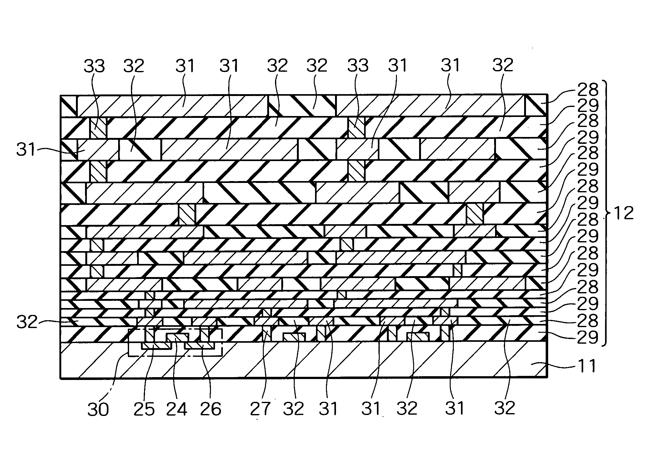
[0048] As shown in FIG. 6, the minute wiring structure portion of the semiconductor device of this embodiment 12 are obtained by alternately laminating insulating layers 29 and wiring layers 28. Specifically, an insulating layer 29 is formed so as to cover the MOS transistor 30 and a surface of the semiconductor substrate 11, and a wiring layer 28 is formed on the insulating layer 29. The wiring layer 28 comprises plural wires 31 and insulating film 32 for insulating the wires 31 from one another. The wire 31 is electrically connected to the source electrode 25 and the drain electrode 26 by a plug 27 formed in the insulating layer 29. Plural pairs of insulating layers 29 and wiring layers 28 are further alternately laminated on the above wiring layer 28 as the lowermost layer. A via 33 is formed in each insulating layer 29 to mutually connect each wire 31 of the wiring layer 28 provided on the insulating layer 29 concerned to each wire 31 of the wiring layer provided beneath the ins...

first embodiment

[0072] Furthermore, in the semiconductor device of this modification, the area for providing necessary external terminals can be secured, and also the empty area 36 can be provided. Therefore, when another element is mounted, a desired external terminal may be provided in the empty area 36. The operation and effect other than the operation and effect of the semiconductor device of this modification are the same as the semiconductor device of the first embodiment described above.

[0073] Next, a semiconductor device according to a second modification of the first embodiment of the present invention will be described. FIG. 9 is a cross-sectional view showing the semiconductor device according to this modification. In the semiconductor device of the first embodiment described above, the external terminals 19 are provided in the wiring layer 17 serving as the uppermost layer. However, in the semiconductor device of this modification, as shown in FIG. 9, an insulating layer 34 is provided ...

second embodiment

[0083] Next, the effect of examples of the present invention will be described by comparing it with comparison examples out of the range of this invention. In this example, the semiconductor devices, which have the same construction as the first or the present invention, were estimated on the basis of a single package temperature cycle test (−40° C., 30 minutes / +125° C., 30 minutes) by using FCBGA package. The estimating method of the FCBGA package was performed by electrically connecting the semiconductor device to the mount board and measuring the resistance values of the wires by which the mount board and the semiconductor device are connected to each other while a BGA terminal provided on a surface of the mount board on which the semiconductor device is not mounted is set as a measuring point. The temperature cycle test adopted a success condition under which the variation rate of the resistance value at a measuring place is within ±10% until 1000 cycles.

[0084] The FCBG packages...


PUM


Abstract

A minute wiring structure portion including first wiring layers and first insulating layers, in which each of first wiring layers and each of first insulating layers are alternately laminated, is formed on a semiconductor substrate. A first huge wiring structure portion is formed on the minute wiring structure portion, and the first huge wiring structure portion is formed by successively forming on the minute wiring structure portion, in the following order, the first huge wiring portion including second wiring layers has a thickness of twice or more of the thickness of the first wiring layers and second insulating layers, in which each of second wiring layers and each of second wiring layers are alternately laminated, and a second huge wiring structure portion including third wiring layers has a thickness of twice or more of the thickness of the first wiring layer and a third insulating layer in which the elastic modulus at 25° C. is not more than that of the second insulating layers, each of the third wiring layers and each of the third insulating layers being alternately laminated.

Description

BACKGROUND OF THE INVENTION [0001] 1. Field of the Invention [0002] The presents invention relates to a semiconductor device having a huge wiring structure portion on a minute wiring structure portion including wiring layers and insulating layers, each of the wiring layers and each of the insulating layers being alternately laminated, the huge wiring structure portion including wiring layers having thicker than the wiring layer of the minute wiring structure portion and insulating layers having thicker than the insulating layer of the minute wiring structure portion, and the wiring layers and the insulating layers of the huge wiring structure portion being alternately laminated. [0003] 2. Description of the Related Art [0004] In connection with miniaturization and highly functional design of electronic equipment, miniaturization and high densification of wirings have been recently required of semiconductor chips. For example, in a microprocessor designed on the basis of the 130 nm r...

Claims


Application Information

Patent Timeline
Patent Type & Authority Applications(United States)
IPC IPC(8): H01L23/12
CPCH01L23/3114H01L23/528H01L23/5286H01L2924/3011H01L2924/0002H01L2924/00
Inventor KIKUCHI, KATSUMIYAMAMICHI, SHINTAROMURAI, HIDEYAHONDA, HIROKAZUSOEJIMA, KOJIMIYAZAKI, SHINICHI
Owner RENESAS ELECTRONICS CORP
Why Eureka
Try Eureka