Light emitting device having vertically stacked light emitting diodes

a technology of light emitting diodes and light emitting diodes, which is applied in the manufacturing of semiconductor/solid-state devices, semiconductor devices, electrical devices, etc., can solve the problems of increasing manufacturing costs per chip, limited improvement of light extraction efficiency, and led not continuously emitting light, so as to improve light output and improve light output. per unit area

Active Publication Date: 2010-09-02
SEOUL VIOSYS CO LTD
View PDF15 Cites 18 Cited by
  • Summary
  • Abstract
  • Description
  • Claims
  • Application Information

AI Technical Summary

Benefits of technology

[0034]According to the embodiments of the present invention, there is provided a light emitting diode capable of improving light output per unit area using vertically stacked light emitting diodes. Further, there is provided a light emitting device which emits light with a plurality of wavelengths by forming active layers of the vertically stacked light emitting diodes with different materials. Furthermore, there is provided a light emitting device with improved light output which can be driven under an AC power supply by electrically connecting a plurality of light emitting cells having vertically stacked light emitting diodes.

Problems solved by technology

However, since there is a limitation in improvement of the light extraction efficiency, a chip area should be increased in order to obtain necessary light output per unit chip.
The increase in the chip area results in the increase in manufacturing costs per chip.
Thus, in a case where the LED is used while connecting directly to the AC power supply, there is a problem in that the LED does not continuously emit light and may be easily damaged due to reverse current.
In such a light emitting device, since LED arrays are alternately operated under an AC power supply, its light output is considerably limited as compared with a case where light emitting cells are simultaneously operated.

Method used


Image

  • Light emitting device having vertically stacked light emitting diodes
  • Light emitting device having vertically stacked light emitting diodes
  • Light emitting device having vertically stacked light emitting diodes

Examples


Embodiment Construction

[0044]Hereinafter, preferred embodiments of the present invention will be described in detail with reference to the accompanying drawings. The following embodiments are provided as an illustration to fully convey the spirit of the present invention to those skilled in the art. Thus, the present invention is not limited to the embodiments which will be described below, but may be implemented in other forms. In the drawings, the width, length, thickness, etc. of components may be exaggerated for the sake of convenience. Throughout the descriptions, like reference numerals designate like elements.

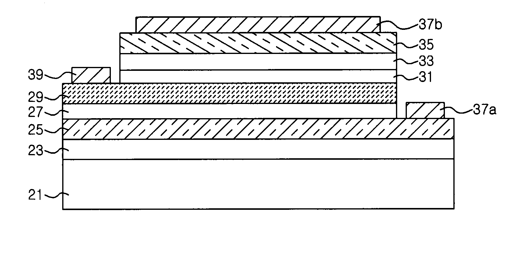
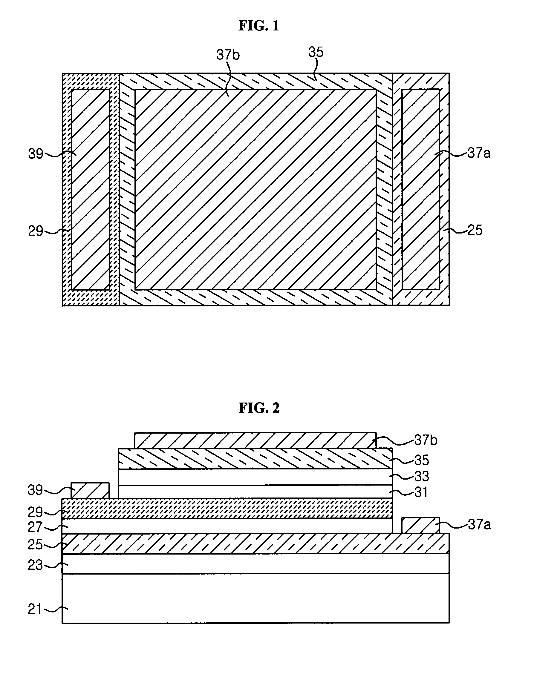
[0045]FIGS. 1 and 2 are plan and sectional views illustrating an embodiment of a light emitting device according to an aspect of the present invention, respectively.

[0046]Referring to FIGS. 1 and 2, a lower N-type semiconductor layer 25 is positioned on a substrate 21. For example, the substrate 21 may be a sapphire substrate, SiC substrate or the like. A buffer layer 23 may be interposed betw...


PUM


Abstract

Disclosed is a light emitting device having vertically stacked light emitting diodes. It comprises a lower semiconductor layer of a first conductive type positioned on a substrate, a semiconductor layer of a second conductive type on the lower semiconductor layer of a first conductive type, and an upper semiconductor layer of a first conductive type on the semiconductor layer of a second conductive type. Furthermore, a lower active layer is interposed between the lower semiconductor layer of a first conductive type and the semiconductor layer of a second conductive type, and an upper active layer is interposed between the semiconductor layer of a second conductive type and the upper semiconductor layer of a first conductive type. Accordingly, there is provided a light emitting device having a structure in which a lower light emitting diode comprising the lower active layer and an upper light emitting diode comprising the upper active layer are vertically stacked. Therefore, light output per unit area of the light emitting device is enhanced as compared with a conventional light emitting device, and thus, a chip area of the light emitting device needed to obtain the same light output as the conventional light emitting device can be reduced.

Description

CROSS REFERENCE TO RELATED APPLICATIONS[0001]This application is a divisional of U.S. patent application Ser. No. 12 / 064,228 filed Feb. 19, 2008 which is the National Stage Entry of International Application No. PCT / KR2006 / 003844 filed Sep. 27, 2006 and claims priority from Korean Patent Application No. 2005-0103201 filed Oct. 31, 2005 and Korean Patent Application No. 2005-0091998 filed Sep. 30, 2005, which are hereby incorporated by reference for all purposes as if fully set forth herein.TECHNICAL FIELD[0002]The present invention relates a light emitting device, and more particularly, to a light emitting device having vertically stacked light emitting diodes.BACKGROUND ART[0003]GaN-based light emitting diodes (LEDs) have been applied and developed for about 10 years. The GaN-based LEDs have significantly advance the LED technologies and has been employed in various applications including full color LED displays, LED traffic signals, white LEDs and the like.[0004]Recently, high-eff...

Claims


Application Information

Patent Timeline
Patent Type & Authority Applications(United States)
IPC IPC(8): H01L27/15H01L33/02H01L33/08H01L33/26
CPCH01L27/153H01L33/08
Inventor KIM, SUNG HANKIM, KYOUNG HOON
Owner SEOUL VIOSYS CO LTD
Why Eureka
Try Eureka