Semiconductor device

a technology of semiconductors and devices, applied in the direction of semiconductor devices, basic electric elements, electrical equipment, etc., can solve the problems of generating crystal defects, affecting the reliability of elements, and fluctuating properties,

Active Publication Date: 2010-09-16
KK TOSHIBA
View PDF4 Cites 47 Cited by
  • Summary
  • Abstract
  • Description
  • Claims
  • Application Information

AI Technical Summary

Problems solved by technology

If the electric field may be intensified due to the concentrated electric field, electrons accelerated by the high electric field are injected into a passivation film or an AlGaN layer, thus generating crystal defects.
This results in a problem in that the properties fluctuate and the reliabilities of the element deteriorate.
However, this method has a disadvantage in that a larger number of times of depositing insulating films may increase fluctuations in properties due to variations in their film thicknesses.
Furthermore, this method may raise a problem in that, if the insulating films become too thick, a film stress is increased and thus cracks generate in the insulating films, resulting in deteriorations in reliability.

Method used


Image

  • Semiconductor device
  • Semiconductor device
  • Semiconductor device

Examples


first embodiment

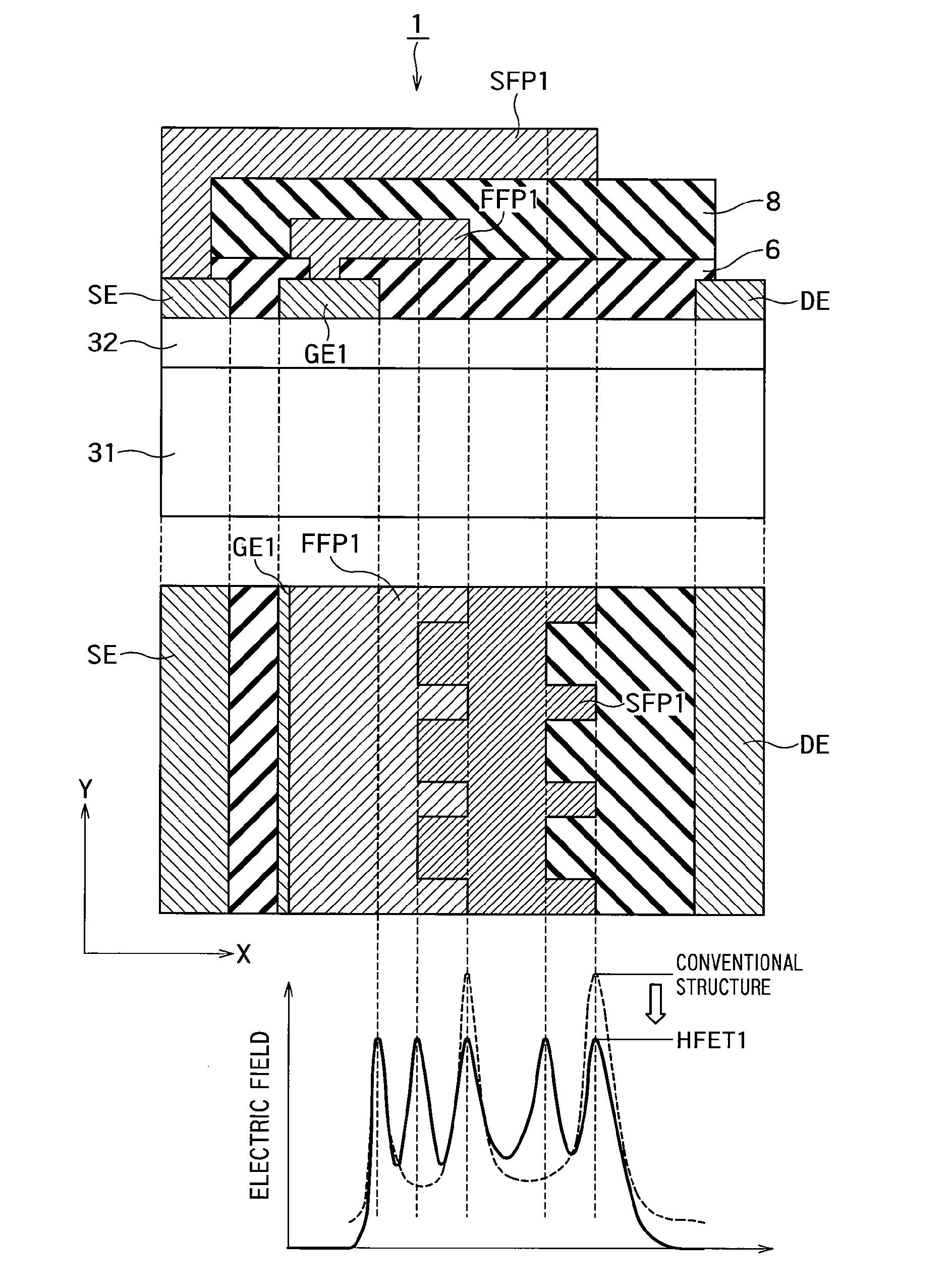
[0033]FIG. 1 shows the outlined constitution of a GaN-HFET according to the first embodiment of the present invention.

[0034]As shown in an outlined cross-sectional view at the upper part in FIG. 1, a GaN-HFET1 in the present embodiment includes a channel layer 31, a barrier layer 32, a source electrode SE, a drain electrode DE, a gate electrode GE1, insulating films 6 and 8, and field plate electrodes FFP1 and SFP1.

[0035]The channel layer 31 is formed of a non-doped GaN layer and corresponds to, for example, a first semiconductor layer in the present embodiment. The barrier layer 32 is formed of a non-doped AlGaN layer on the channel layer 31 and corresponds to, for example, a second semiconductor layer in the present embodiment. The gate electrode GE1 is formed on the barrier layer 32 in such a manner as to provide a Schottky contact between itself and the barrier layer 32. The gate electrode GE1 corresponds to, for example, a first electrode in the present embodiment. The source e...

second embodiment

(2) Second Embodiment

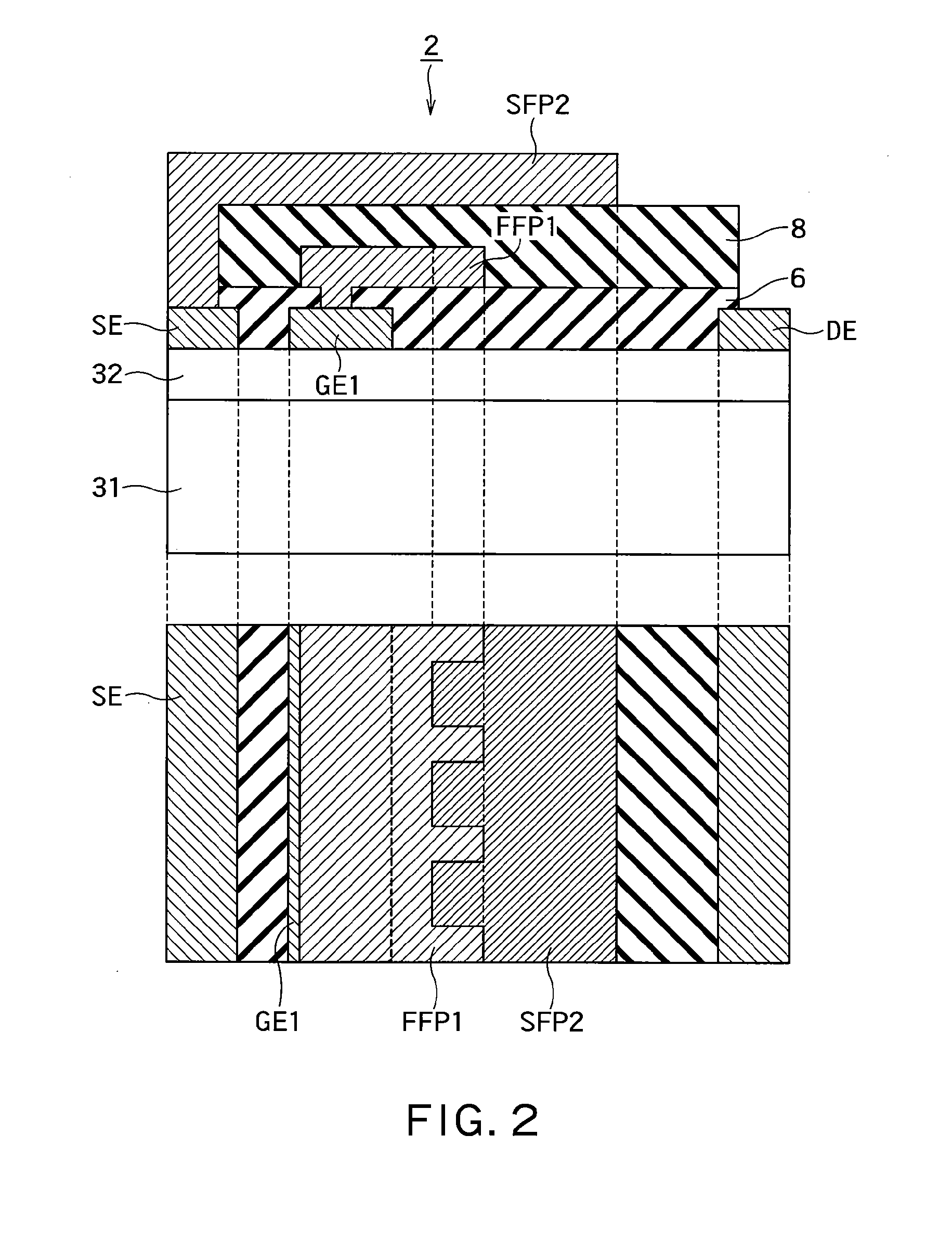
[0045]FIG. 5 shows the outlined constitution of a GaN-HFET according to the second embodiment of the present invention. The second through sixth embodiments will be described only on their differences from the first embodiment.

[0046]As may be clear from comparison to FIG. 1, a first feature of a GaN-HFET4 in the present embodiment is that the amount of the change “e” in length of the field plate electrode FFP1 is smaller than the amount of the change “f” in length of a field plate electrode SFP4 (e1 and SFP4, a more relaxed electric field distribution can be obtained.

[0047]Further, a second feature of a GaN-HFET4 is that the total sum “h” of the thicknesses of insulating films 6 and 8 under the field plate electrode SFP4 is larger than the thickness “g” of the insulating film 6 under the field plate electrode FFP1 (g1 and SFP4, the peak of the electric field can be lowered further. Preferably, a ratio e / f of the changes in length between the field plate electrod...

third embodiment

(3) Third Embodiment

[0048]FIG. 7 shows the outlined constitution of a GaN-HFET according to a third embodiment of the present invention.

[0049]As may be clear from comparison to FIG. 5, the feature of a GaN-HFET6 in the present embodiment is that X-directional lengths of the respective field plate electrodes FFP1 and SFP6 change in a period common to them but in phases different from each other. By using such a structure, an electric field is securely concentrated on dispersed positions, so that its peak can be lowered further. Although FIG. 7 has shown such a structure that one phase might shift by half the other period, the present invention is not limited to it; for example, almost the same effects can be obtained as long as one phase shifts even by the quarter of the other period.


PUM


Abstract

A semiconductor device includes: a first semiconductor layer of non-doped AlXGa1-XN (0≦X<1); a second semiconductor layer of non-doped or n-type AlYGa1-YN (0<Y≦1, X<Y) on the first semiconductor layer; a first electrode on the second semiconductor layer; a second electrode on the second semiconductor layer that is separated from the first electrode and electrically connected to the second semiconductor layer; a first insulating film covering the first and second electrodes; a first field plate electrode electrically connected to the first electrode and covered by a second insulating film; and a second field plate electrode on the second insulating film, wherein a length of at least one of the first and second field plate electrodes in a first direction from the first electrode toward the second electrode changes periodically in a second direction intersecting the first direction.

Description

CROSS REFERENCE TO RELATED APPLICATIONS[0001]This application claims benefit of priority under 35 USC §119 to Japanese Patent Application No. 2009-061209, filed on Mar. 13, 2009, the contents of which are incorporated by reference herein.BACKGROUND OF THE INVENTION[0002]1. Field of the Invention[0003]The present invention relates to a semiconductor device.[0004]2. Related Background Art[0005]A power semiconductor element such as a switching element or a diode is used in circuits such as a switching power supply and an inverter and desired to have such properties as a high breakdown voltage and a low turn on-resistance.[0006]However, the breakdown voltage and the turn on-resistance are in a relationship of trade-off, which is determined by a material of the element. The main element material, silicon, has already reached almost its limits of low turn on-resistance by the past progresses in technological development. Therefore, in order to further lower the turn on-resistance, any oth...

Claims


Application Information

Patent Timeline
Patent Type & Authority Applications(United States)
IPC IPC(8): H01L27/06
CPCH01L29/0692H01L29/2003H01L29/7787H01L29/41725H01L29/42316H01L29/402H01L29/205H01L29/404H01L29/872
Inventor SAITO, WATARU
Owner KK TOSHIBA
Why Eureka
Try Eureka