


Quick Research
Generate reliable direction feasibility study reports for your R&D in just a few steps.

Technical Q&A
Discover and master advanced knowledge NOW. Basics, ideas, possibilities, all at once.

Find Solutions
As an expert in R&D theories, this can generate solutions to your technical problems instantly.

Evaluate Feasibility
Analyze your overall solution with one click, know your potential R&D risks in advance.

Monitor Landscape
Get weekly tech updates, stay abreast of the latest tech innovations and key insights.
Semiconductor device and layout method therefor
a technology of semiconductor devices and layout methods, applied in semiconductor devices, semiconductor/solid-state device details, capacitors, etc., can solve the problems of increasing time and cost, inability to perform characteristics evaluation, etc., and achieve the effect of efficient evaluation
- Summary
- Abstract
- Description
- Claims
- Application Information
AI Technical Summary
Benefits of technology
Problems solved by technology
Method used
Image

Examples
first exemplary embodiment
[0026][First Exemplary Embodiment]
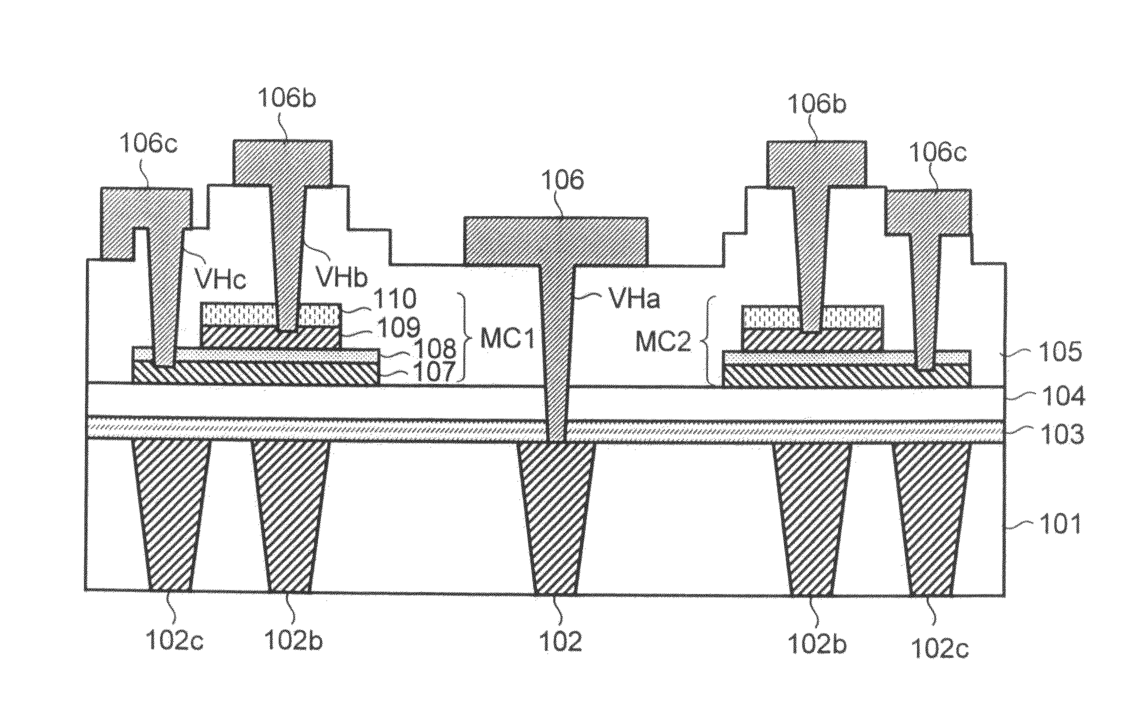
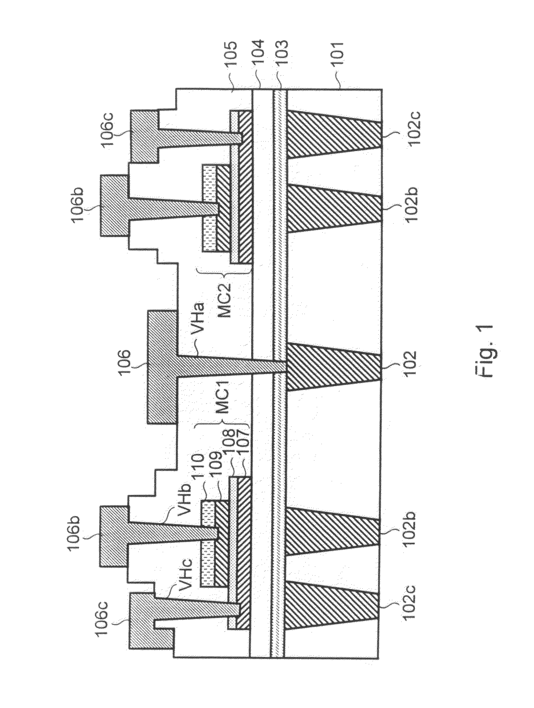
[0027]FIG. 1 is a schematic cross-section view illustrating a semiconductor device according to a first exemplary embodiment of the present invention. The semiconductor device includes a first interlayer insulating film 101, lower wiring lines 102, a cap layer 103, a second interlayer insulating film 104, a third interlayer insulating film 105, upper wiring lines 106, and MIM capacitors MC1 and MC2. The MIM capacitors MC1 and MC2 each include a lower electrode 107, a capacitor insulating film 108, an upper electrode 109, and a hard mask layer 110.
[0028]As shown in FIG. 1, the first interlayer insulating film 101 is composed of Si02, for example, and includes the lower wiring lines 102 composed of Cu, for example. On the first interlayer insulating film 101, the cap layer 103, which is composed of SiC, SiCN, or SiN with about 70-100 nm thickness, for example, is formed. On the cap layer 103, the second interlayer insulating film 104 composed of SiO2 ...
second exemplary embodiment
[0044][Second Exemplary Embodiment]
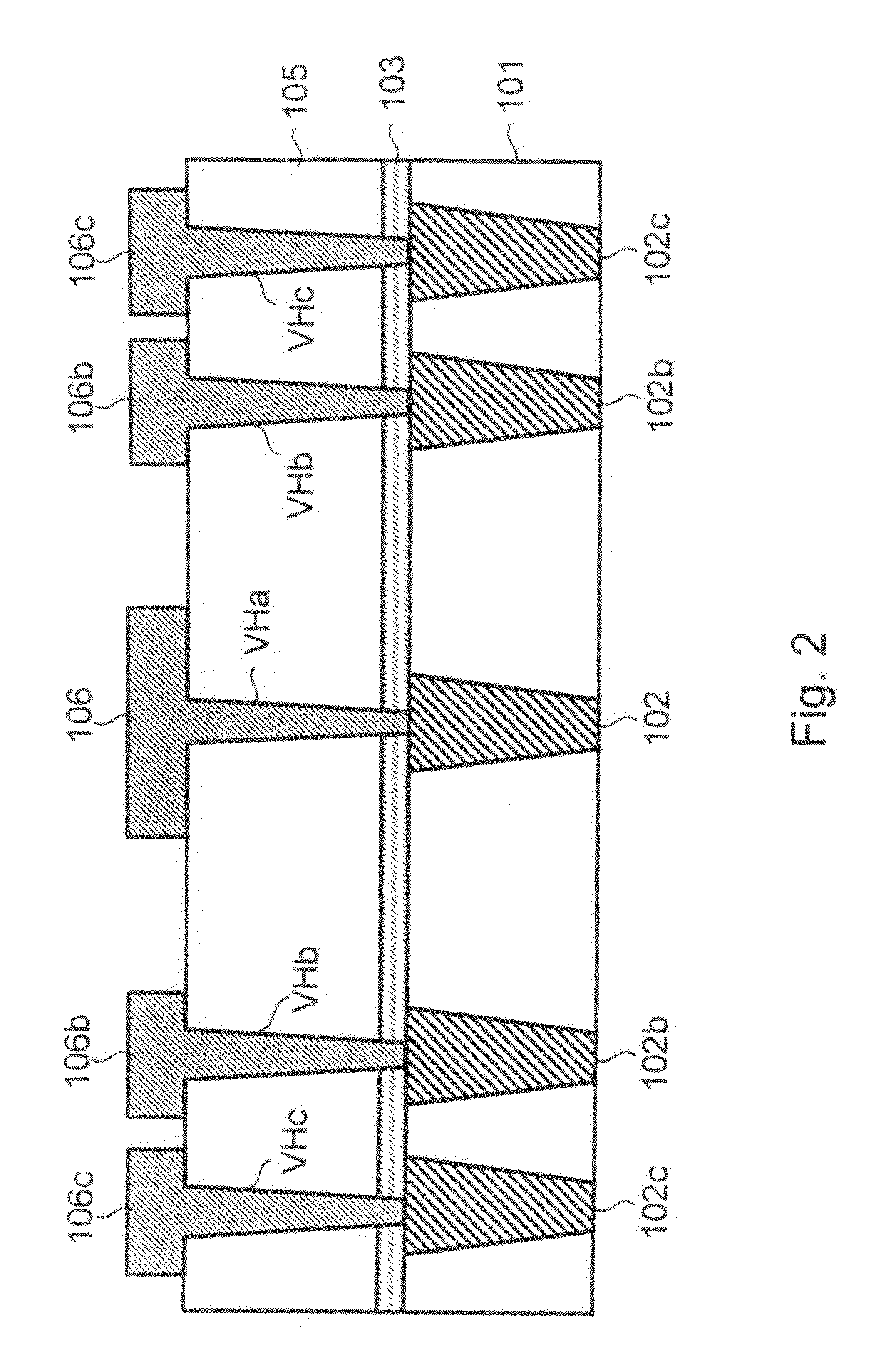
[0045]Next, a second exemplary embodiment of the present invention will be described with reference to FIG. 7. FIG. 7 is a plan layout diagram illustrating a semiconductor device according to the second exemplary embodiment of the present invention. As with FIG. 4, FIG. 7 shows a position relation among the lower wiring line 102, the lower electrode 107, the upper electrode 109, and the via holes VHa, VHb, and VHc.
[0046]In the semiconductor device according to the second exemplary embodiment of the present invention, only evaluation circuits of MIM capacitors are formed. Therefore, there is no need to take into consideration the voltage difference between the lower wiring lines 102 and the via holes VHb or VHc. Here, the lower wiring lines 102 connect to the via holes VHb and VHc in the case of mounting no MIM capacitor. Therefore, it is possible to arrange the via holes VHa, which directly connect the lower wiring lines 102 to the upper wiring lin...
PUM
 Abstract
Description
Claims
Application Information
 - R&D Engineer
- R&D Manager
- IP Professional
- Industry Leading Data Capabilities
- Powerful AI technology
- Patent DNA Extraction
Browse by: Latest US Patents, China's latest patents, Technical Efficacy Thesaurus, Application Domain, Technology Topic, Popular Technical Reports.
© 2024 PatSnap. All rights reserved.Legal|Privacy policy|Modern Slavery Act Transparency Statement|Sitemap|About US| Contact US: help@patsnap.com