Formation Of Raised Source/Drain On A Strained Thin Film Implanted With Cold And/Or Molecular Carbon

a thin film, cold and/or molecular carbon technology, applied in the direction of basic electric elements, electrical equipment, semiconductor devices, etc., can solve the problems of loss of strain caused by source/drain implantation, defects in silicon substrates, and reduced overall yield, so as to enhance stress in the channel region and stress in the source or drain region.

Inactive Publication Date: 2010-11-04
VARIAN SEMICON EQUIP ASSOC INC
View PDF6 Cites 17 Cited by
  • Summary
  • Abstract
  • Description
  • Claims
  • Application Information

AI Technical Summary

Benefits of technology

The patent describes methods for enhancing stress in a semiconductor device by forming strain layers and raised source/drain regions. The strain layers are formed by ion-implantation with cold carbon or molecular carbon ions, which create latent strain in the device. A silicon layer is then deposited over the strain layers, and the raised source/drain regions are doped and annealed to activate them. The methods improve the performance of semiconductor devices by enhancing their ability to withstand stress and improving their performance in high-speed applications.

Problems solved by technology

The technical problem addressed in this patent text is the loss of strain in transistor structures caused by subsequent source/drain implantation steps and traditional carbon-implant techniques, which can result in reduced overall yield. There is a need for a simple and efficient method to impart and maintain strain in these structures to maximize device yields.

Method used


Image

  • Formation Of Raised Source/Drain On A Strained Thin Film Implanted With Cold And/Or Molecular Carbon
  • Formation Of Raised Source/Drain On A Strained Thin Film Implanted With Cold And/Or Molecular Carbon
  • Formation Of Raised Source/Drain On A Strained Thin Film Implanted With Cold And/Or Molecular Carbon

Examples


Embodiment Construction

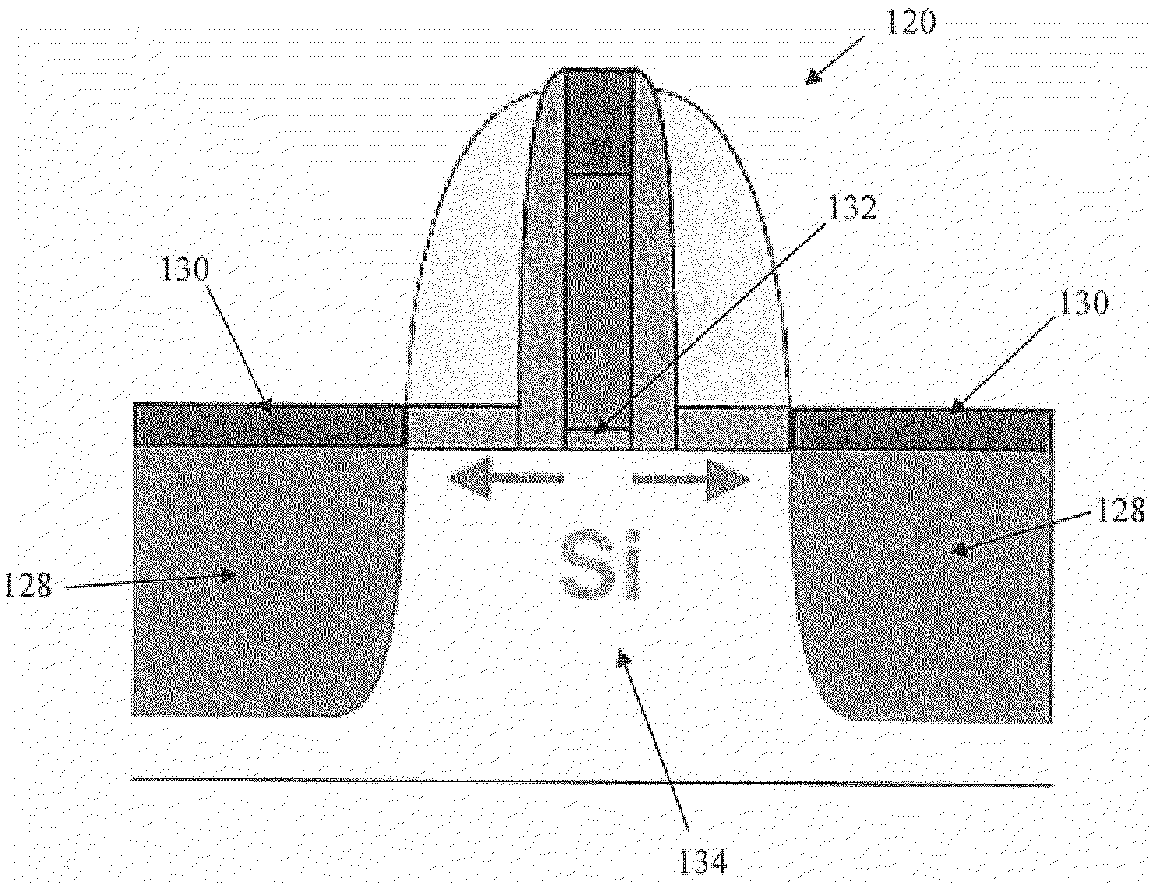
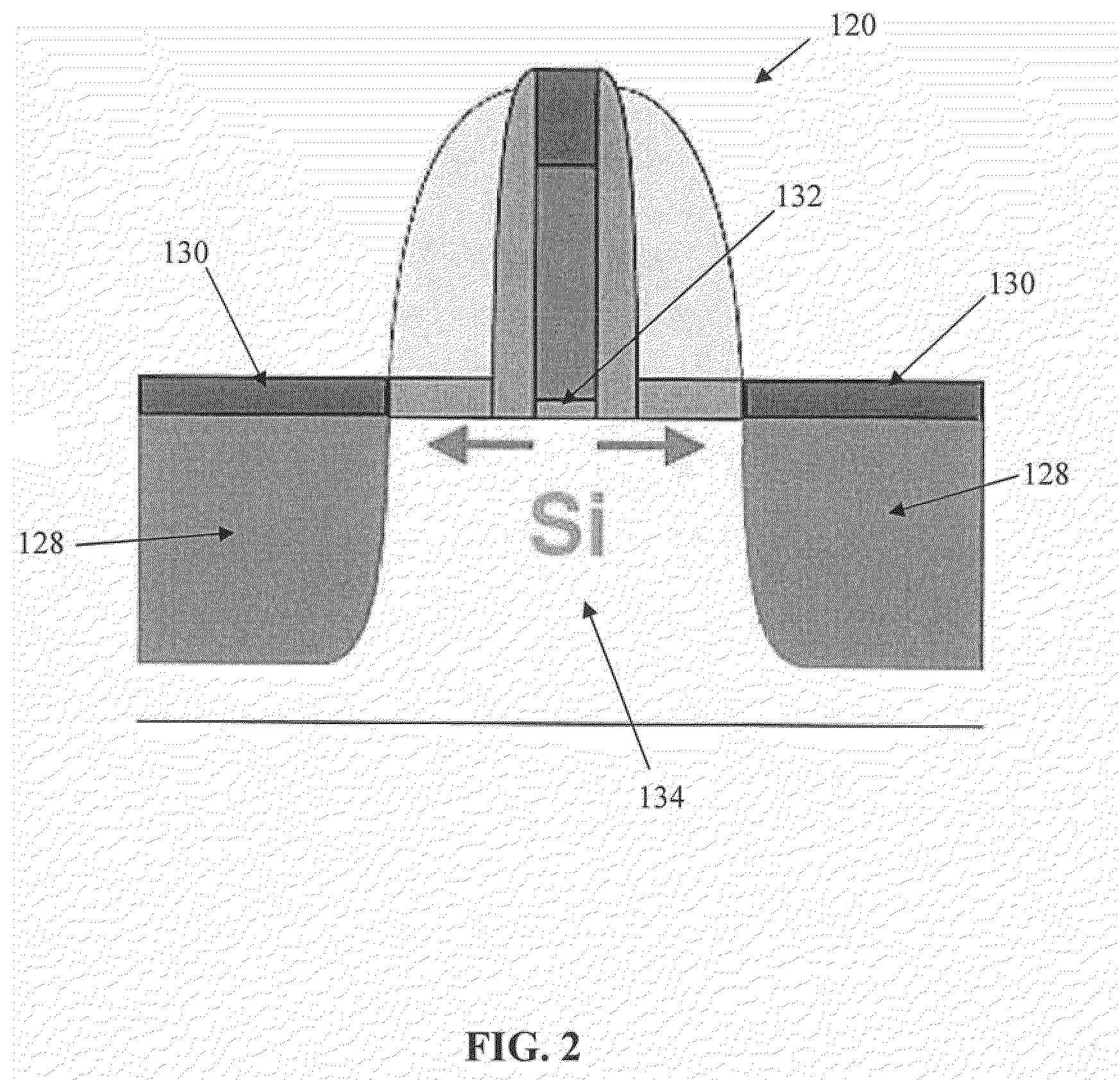
[0017]A technique is disclosed for combating the aforementioned loss of strain problem is to grow a raised Source / Drain (S / D) on top of the Si—C layer. Cold ion implantation of carbon and / or molecular carbon ion implantation enable the creation of an Si—C layer that can then be used as the base for a raised S / D. And since the S / D are raised above the Si—C layer, subsequent implantation of dopant ions (e.g., P, As) in the raised S / D regions has less impact on the strain layer (i.e., the dopant implant will not relax the strain layer) as compared to implants in the C-containing regions. In addition, the use of cold implantation of carbon results in a substrate surface having fewer defects than is found using traditional carbon implantation techniques, thus resulting in a better surface upon which to subsequently grow the raised S / D regions.

[0018]The disclosed technique includes a single or series of carbon ion implants at a reduced temperature and / or using molecular carbon with or wit...


PUM


Abstract

A method is disclosed for enhancing tensile stress in the channel region of a semiconductor structure. The method includes performing one or more cold-carbon or molecular carbon ion implantation steps to implant carbon ions within the semiconductor structure to create strain layers on either side of a channel region. Raised source/drain regions are then formed above the strain layers, and subsequent ion implantation steps are used to dope the raised source/drain region. A millisecond anneal step activates the strain layers and the raised source/drain regions. The strain layers enhances carrier mobility within a channel region of the semiconductor structure, while the raised source/drain regions minimize reduction in strain in the strain layer caused by subsequent implantation of dopant ions in the raised source/drain regions.

Description


Claims


Application Information

Patent Timeline
Owner VARIAN SEMICON EQUIP ASSOC INC
Why Eureka
Try Eureka