Building block for a secure CMOS logic cell library

a technology of logic cell library and building block, which is applied in the direction of logic circuits, logic circuits, logic circuits characterised by logic functions, etc., can solve problems such as inability to find

Active Publication Date: 2010-12-02
RAMBUS INC +1
View PDF48 Cites 26 Cited by
  • Summary
  • Abstract
  • Description
  • Claims
  • Application Information

AI Technical Summary

Benefits of technology

[0008]A logical circuit is described. In one embodiment, the logical circuit comprises a first logic input, a second logic input, a control input for implementing a plurality of logical functions, and a logic output, wherein the logic circuit is configured to implement a plurality of logical functions according to the control input, where the state of the control input is controlled by camouflaged circuitry.

Problems solved by technology

One attempting to reverse engineer an ASIC designed with logic gates as described herein faces a large number of identical circuit blocks and will not be able to find any obvious clue for logic function identification.

Method used


Image

  • Building block for a secure CMOS logic cell library
  • Building block for a secure CMOS logic cell library
  • Building block for a secure CMOS logic cell library

Examples


Embodiment Construction

[0023]In the following description, reference is made to the accompanying drawings which form a part hereof, and which is shown, by way of illustration, several embodiments of the present invention. It is understood that other embodiments may be utilized and structural changes may be made without departing from the scope of the present invention.

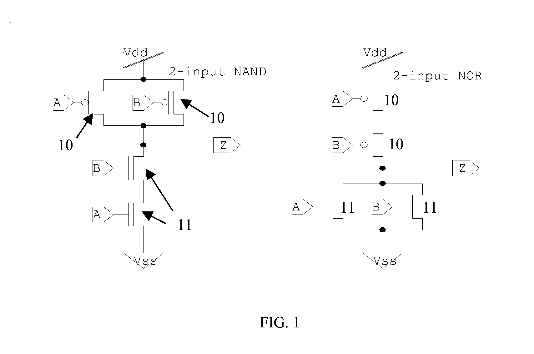
[0024]The schematics of a standard 2-input NAND gate and a 2-input NOR gate are shown in FIG. 1 where 10 refers to P devices and 11 refers to N devices. Reverse engineers can use this valuable information to identify the function of each logic gate and thus are able to extract the complete ASIC design. Reverse engineering of an ASIC designed with logic gates implemented by the method of this invention will face a large number of identical circuit blocks and will not be able to find any obvious clue for logic function identification.

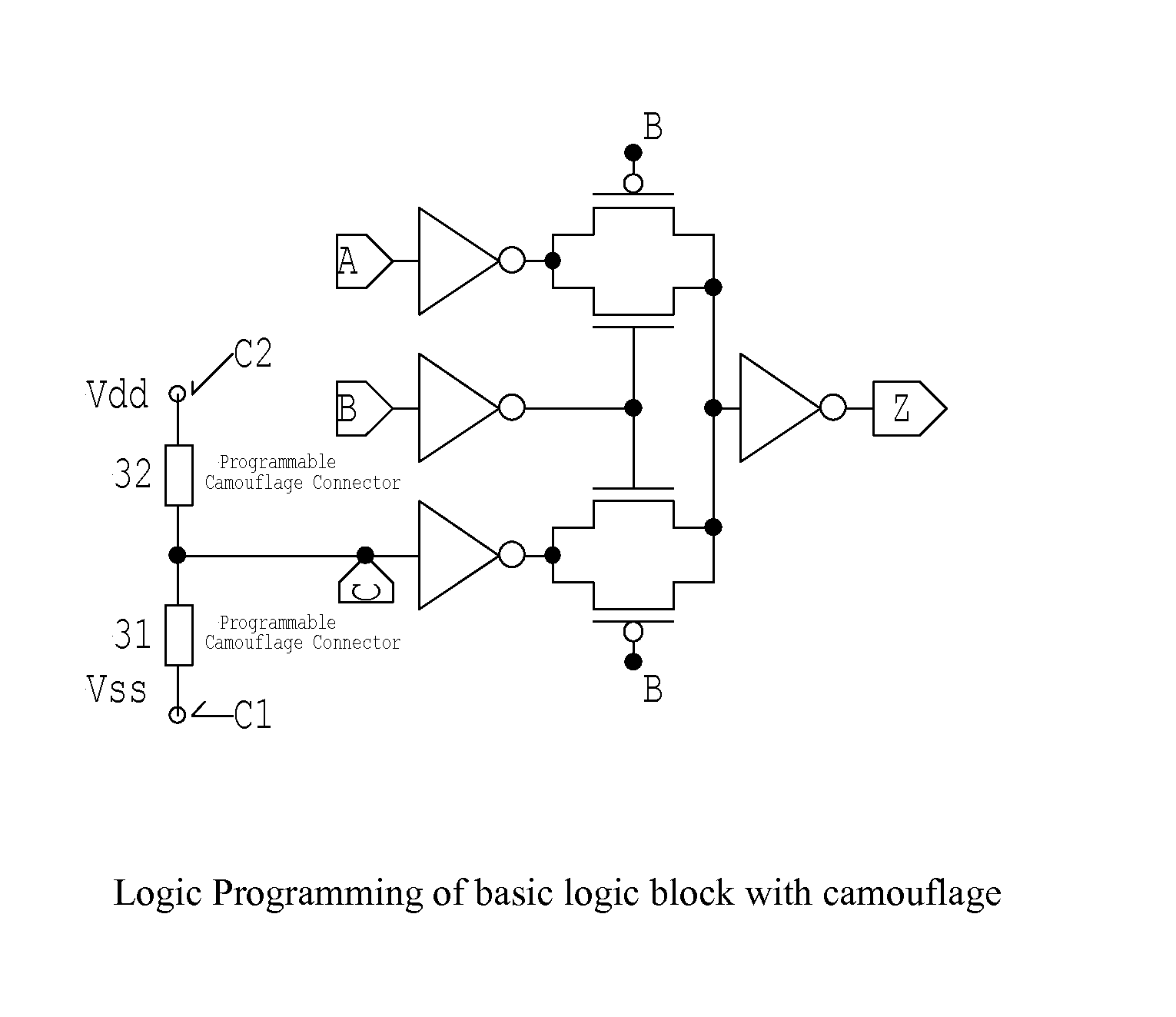
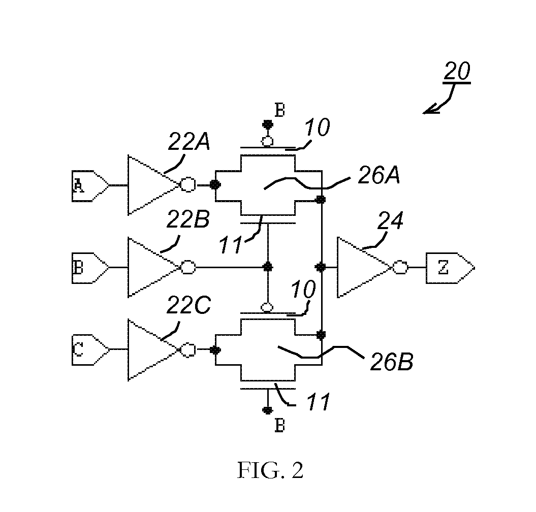
[0025]FIG. 2 shows the schematic of one embodiment the basic logic building block 20, which has three inputs A,...


PUM


Abstract

A logical building block and method of using the building block to design a logic cell library for CMOS (Complementary Metal Oxide Silicon) ASICs (Application Specific Integrated Circuits) is disclosed. Different logic gates, built with the same building block as described in this invention, will have the same schematics of transistor connection and also the same physical layout so that they appear to be physically identical under optical or electron microscopy. An ASIC designed from a library of such logic cells is strongly resistant to a reverse engineering attempt.

Description

CROSS-REFERENCE TO RELATED APPLICATIONS[0001]This application claims benefit of U.S. Provisional Patent Application Ser. No. 61 / 181,930, entitled “BUILDING BLOCK FOR A SECURE CMOS LOGIC CELL LIBRARY,” filed May 28, 2009, by Ronald P. Cocchi, James P. Baukus, Bryan J. Wang, Lap Wai Chow, and Paul Ouyang, which application is hereby incorporated by reference herein.[0002]This application is also related to U.S. patent application Ser. No. 12 / 578,441, entitled “METHOD AND APPARATUS FOR CAMOUFLAGING A STANDARD CELL BASED INTEGRATED CIRCUIT,” by Lap Wai Chow, James P. Baukus, Bryan J. Wang, and Ronald P. Cocchi, filed Nov. 10, 2009, which is a continuation-in-part of U.S. patent application Ser. No. 12 / 380,094, filed Feb. 24, 2009 and entitled “METHOD AND APPARATUS FOR CAMOUFLAGING A PRINTED CIRCUIT BOARD,” by Lap Wai Chow, James P. Baukus, Bryan J. Wang, and Ronald P. Cocchi, which applications are incorporated by reference herein.BACKGROUND OF THE INVENTION[0003]1. Field of the Inventi...

Claims


Application Information

Patent Timeline
Patent Type & Authority Applications(United States)
IPC IPC(8): H03K19/0948H03K19/094
CPCH03K19/20
Inventor COCCHI, RONALD P.BAUKUS, JAMES P.WANG, BRYAN J.CHOW, LAP WAIOUYANG, PAUL
Owner RAMBUS INC
Why Eureka
Try Eureka