Method for forming and integrating metal gate transistors having self-aligned contacts and related structure

a metal gate transistor and self-aligning technology, applied in the field of semiconductor devices, can solve the problems of increasing the difficulty of ensuring sufficient separation between the gate and the source/drain contact, reducing manufacturing yield, and unfavorable increasing fabrication costs

Inactive Publication Date: 2010-12-23
GLOBALFOUNDRIES INC
View PDF13 Cites 60 Cited by
  • Summary
  • Abstract
  • Description
  • Claims
  • Application Information

AI Technical Summary

Problems solved by technology

However, the integration of metal gates with polysilicon resistors and fuses on a common substrate in a conventional process flow can require a number of additional masking steps, which can undesirably increase fabrication cost.
As a result, it can become increasingly difficult to ensure sufficient separation between the gate and source / drain contacts so as to avoid gate-to-source / drain contact shorts.
As a result, the conventional process flow can cause increased gate-to-source / drain contact shorts as FETs are scaled down in size, thereby undesirably reducing manufacturing yield.

Method used


Image

  • Method for forming and integrating metal gate transistors having self-aligned contacts and related structure
  • Method for forming and integrating metal gate transistors having self-aligned contacts and related structure
  • Method for forming and integrating metal gate transistors having self-aligned contacts and related structure

Examples


Embodiment Construction

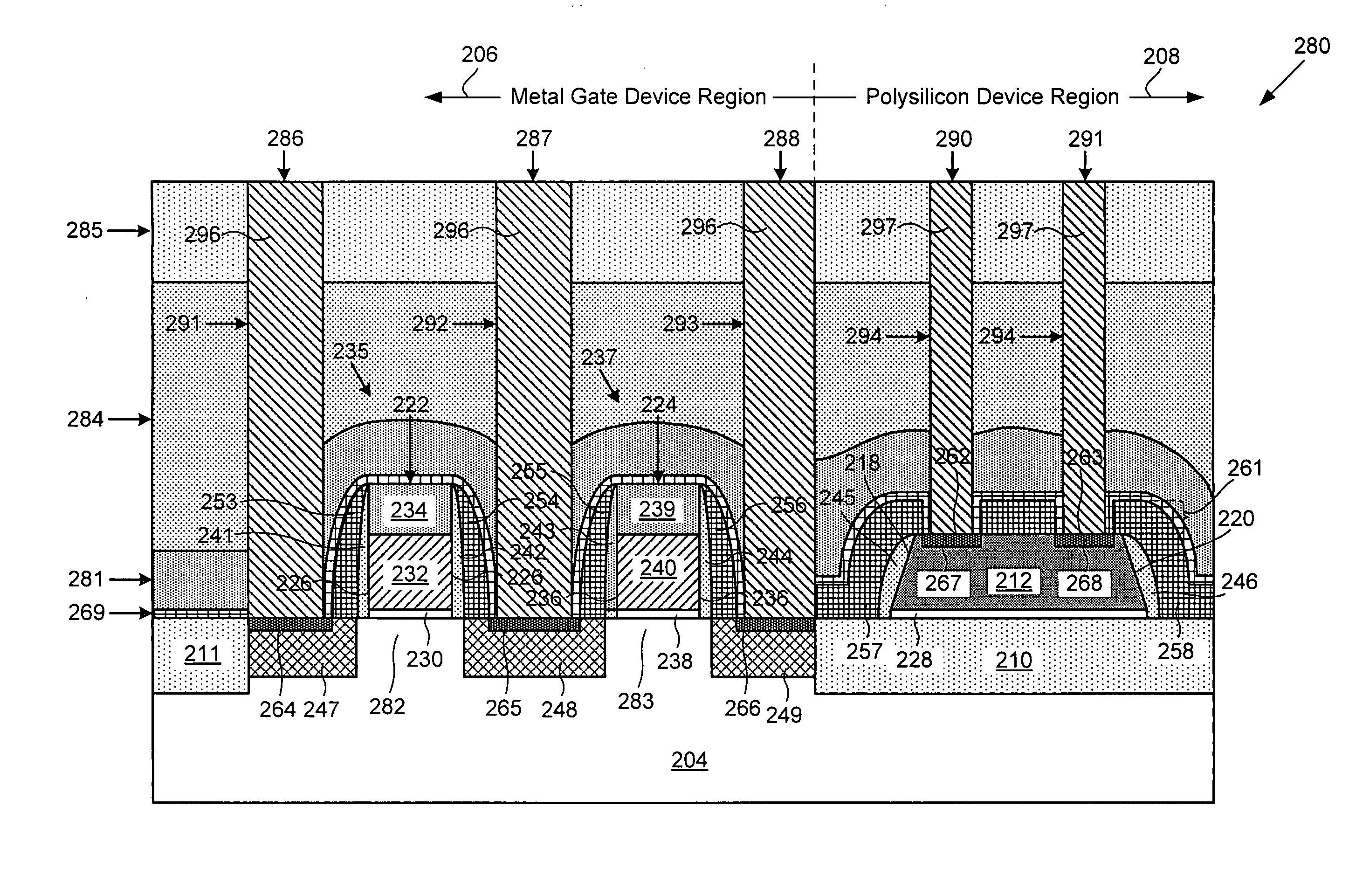
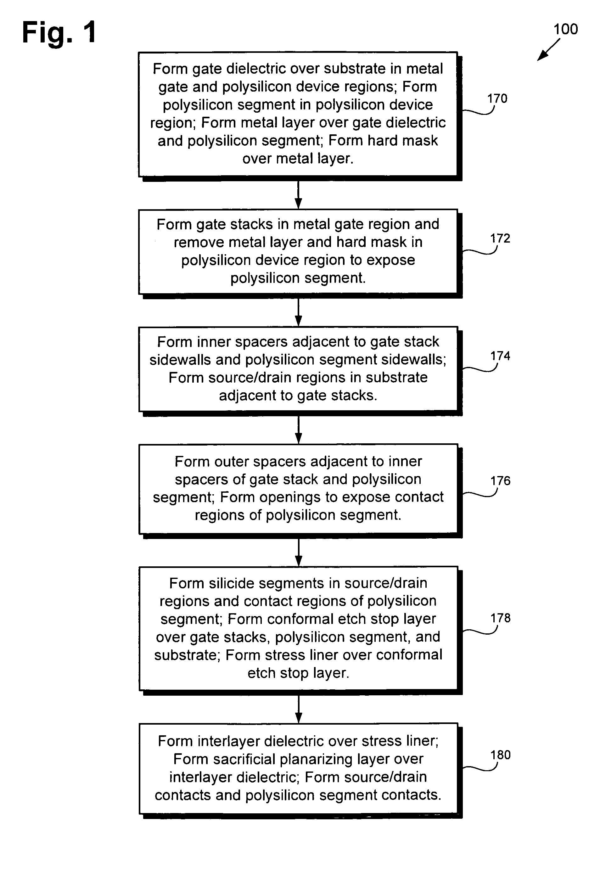
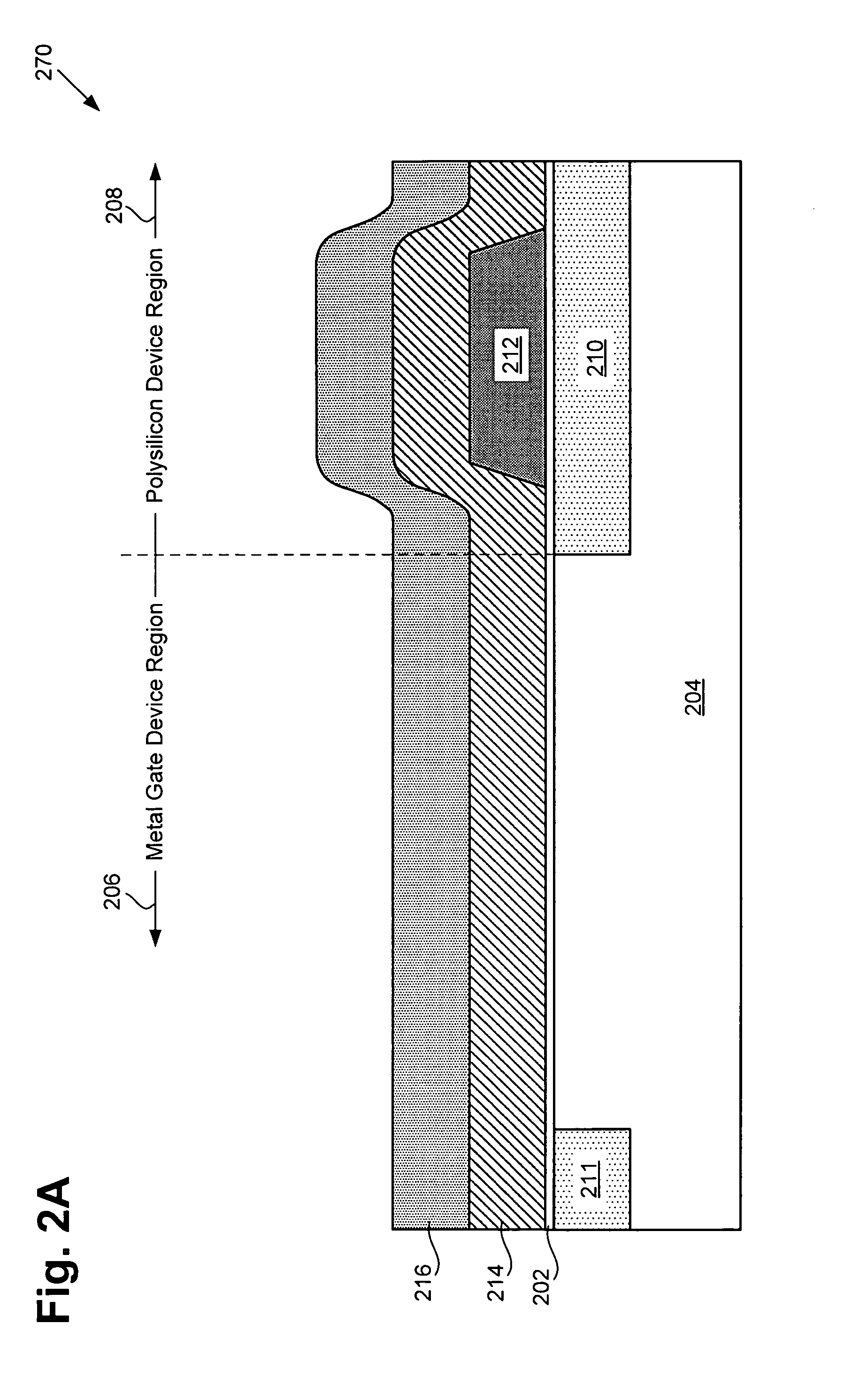
[0013]The present invention is directed to a method for forming and integrating metal gate transistors having self-aligned contacts and related structure. The following description contains specific information pertaining to the implementation of the present invention. One skilled in the art will recognize that the present invention may be implemented in a manner different from that specifically discussed in the present application. Moreover, some of the specific details of the invention are not discussed in order not to obscure the invention.

[0014]The drawings in the present application and their accompanying detailed description are directed to merely exemplary embodiments of the invention. To maintain brevity, other embodiments of the present invention are not specifically described in the present application and are not specifically illustrated by the present drawings. It should be borne in mind that, unless noted otherwise, like or corresponding elements among the figures may b...


PUM


Abstract

According to one exemplary embodiment, a method for forming at least one metal gate transistor with a self-aligned source / drain contact includes forming a metal gate over a substrate. The method further includes forming a source / drain region in the substrate adjacent to the metal gate. The method also includes forming a conformal etch stop layer over the metal gate and the source / drain region. The method further includes forming a source / drain contact over the source / drain region, where the conformal etch stop layer imposes a pre-determined distance between the source / drain contact and the metal gate, thereby causing the source / drain contact to be self-aligned to the metal gate.

Description

TECHNICAL FIELD[0001]The present invention is generally in the field of semiconductors. More particularly, the invention is in the field of semiconductor device fabrication.BACKGROUND ART[0002]Field effect transistors (FETs) that are utilized in semiconductor dies including logic circuits, such as high performance logic circuits, typically require low gate resistance, which can be achieved by utilizing silicided polysilicon gates or metal gates. For logic circuits, it is desirable to integrate FETs with polysilicon devices, such as polysilicon resistors and fuses, on a common substrate. However, the integration of metal gates with polysilicon resistors and fuses on a common substrate in a conventional process flow can require a number of additional masking steps, which can undesirably increase fabrication cost.[0003]As a result of continuing advances in technology, the feature size of FETs utilized in logic circuits, such as high performance logic circuits, continues to scale down, ...

Claims


Application Information

Patent Timeline
Patent Type & Authority Applications(United States)
IPC IPC(8): H01L29/78H01L21/336H01L21/8234
CPCH01L21/28044H01L21/76832H01L21/76834H01L21/76897H01L23/5256H01L29/7843H01L27/0629H01L28/20H01L29/66575H01L29/78H01L27/0617H01L2924/0002H01L2924/00
Inventor KNORR, ANDREAS H.JOHNSON, FRANK SCOTT
Owner GLOBALFOUNDRIES INC
Why Eureka
Try Eureka