Thin film transistor and method of manufacturing the same

a thin film transistor and transistor technology, applied in the direction of transistors, semiconductor devices, electrical equipment, etc., can solve the problems of difficulty in increasing the operation speed of conventional liquid crystal display devices, and achieve the effect of improving characteristics

Active Publication Date: 2008-08-28
SAMSUNG ELECTRONICS CO LTD
View PDF5 Cites 475 Cited by
  • Summary
  • Abstract
  • Description
  • Claims
  • Application Information

AI Technical Summary

Benefits of technology

[0009]Example embodiments may provide a thin film transistor which may have improved characteristics due to improved contact between a source and a drain of the thin film transistor.

Problems solved by technology

If the channel layer of the thin film transistor is an amorphous silicon layer, the charge mobility may be about 0.5 cm2 / Vs, which is low, and thus, it may be difficult to increase the operation speed of the conventional liquid crystal display devices.

Method used


Image

  • Thin film transistor and method of manufacturing the same
  • Thin film transistor and method of manufacturing the same
  • Thin film transistor and method of manufacturing the same

Examples


Embodiment Construction

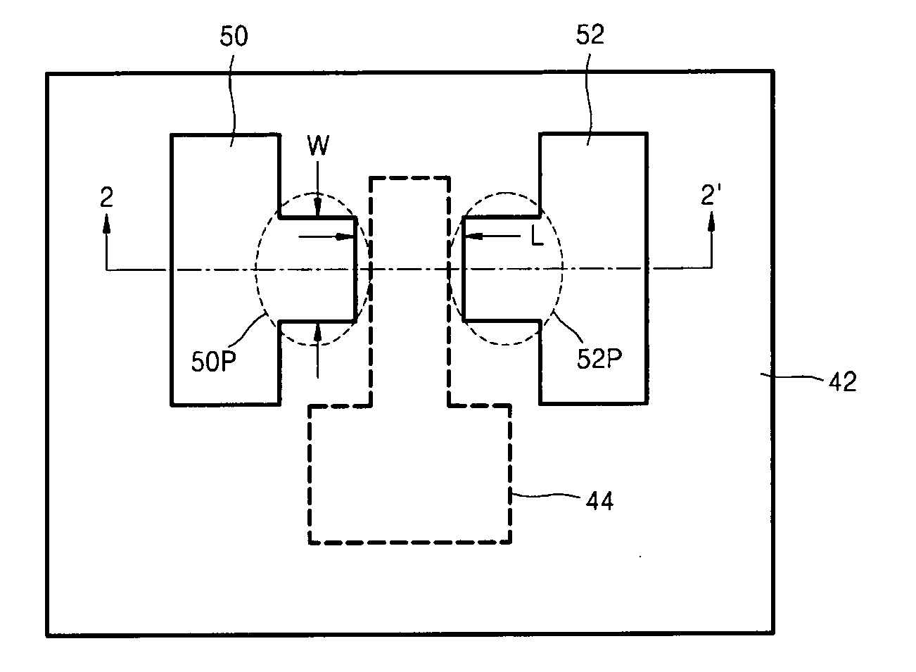
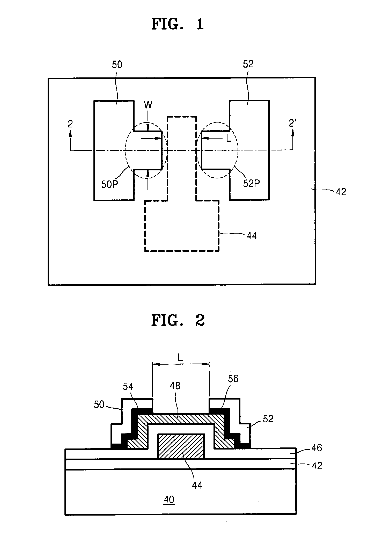
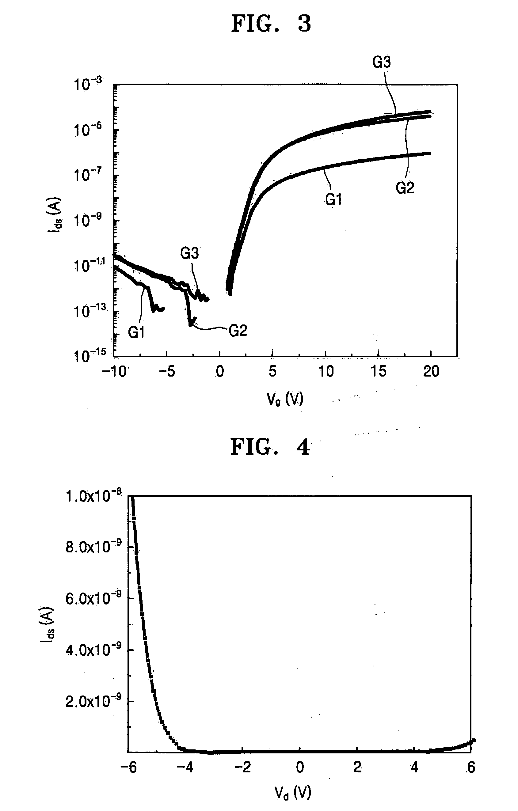
[0048]Detailed example embodiments are disclosed herein. However, specific structural and functional details disclosed herein are merely representative for purposes of describing example embodiments. Example embodiments may, however, be embodied in many alternate forms and should not be construed as limited to only the embodiments set forth herein.

[0049]Accordingly, while example embodiments are capable of various modifications and alternative forms, embodiments thereof are shown by way of example in the drawings and will herein be described in detail. It should be understood, however, that there is no intent to limit example embodiments to the particular forms disclosed, but to the contrary, example embodiments are to cover all modifications, equivalents, and alternatives falling within the scope of example embodiments. Like numbers refer to like elements through the description of the figures.

[0050]It will be understood that, although the terms first, second, etc. may be used here...


PUM

PropertyMeasurementUnit
thicknessaaaaaaaaaa
voltagesaaaaaaaaaa
voltagesaaaaaaaaaa

Abstract

Provided are a thin film transistor and a method of manufacturing the same. The thin film transistor may include a gate; a channel layer; a source and a drain, the source and the drain being formed of metal; and a metal oxide layer, the metal oxide layer being formed between the channel layer and the source and the drain. The metal oxide layer may have a gradually changing metal content between the channel layer and the source and the drain.

Description

PRIORITY STATEMENT[0001]This application claims priority under 35 U.S.C. § 119 to Korean Patent Application No. 10-2007-0020528, filed on Feb. 28, 2007, in the Korean Intellectual Property Office, the entire contents of which are incorporated herein by reference.BACKGROUND[0002]1. Field[0003]Example embodiments relate to a switching device and a method of manufacturing the same, and more particularly, to a thin film transistor and a method of manufacturing the same.[0004]2. Description of Related Art[0005]Thin film transistors may be used as switching devices for flat panel display devices, for example, a liquid crystal display device or an organic light emitting display device.[0006]The mobility or leakage current of a thin film transistor may vary significantly depending on the material and state of a channel layer of the thin film transistor.[0007]The majority of the channel layer of the thin film transistor in conventional liquid crystal display devices may be an amorphous silic...

Claims


Application Information

Patent Timeline
Patent Type & Authority Applications(United States)
IPC IPC(8): H01L29/221H01L21/441H01L29/786
CPCH01L29/7869H01L29/458
Inventor KANG, DONG-HUNGENRIKH, STEFANOVICHSONG, I-HUNPARK, YOUNG-SOOKIM, CHANG-JUNG
Owner SAMSUNG ELECTRONICS CO LTD
Why Eureka
Try Eureka