

Thin film transistor and method of producing thin film transistor
- Summary
- Abstract
- Description
- Claims
- Application Information
AI Technical Summary
Benefits of technology
Problems solved by technology
Method used
Image

Examples
first exemplary embodiment
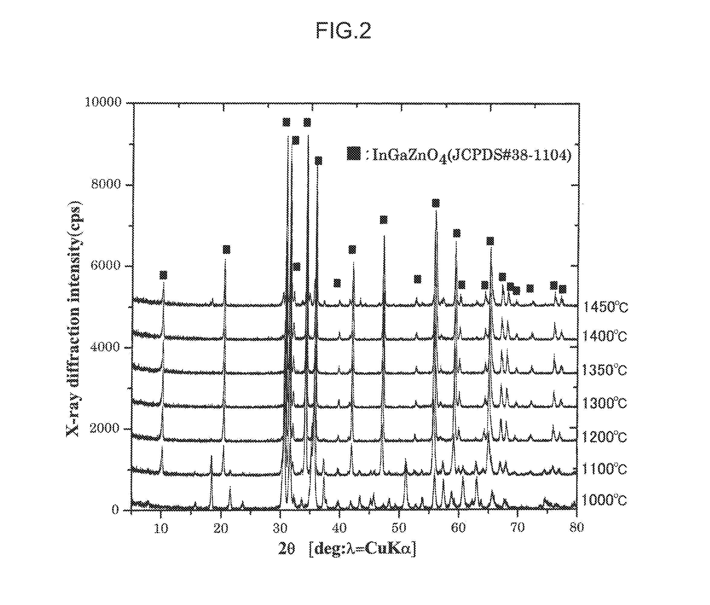
[0038]In the first exemplary embodiment, the IGZO-based oxide material, which is used as a constituent material for the active layer of the TFT according to the invention, is described with reference to the drawings. In the drawings, components having the substantially same function as that of the components that have been previously explained are shown with the same symbol, and explanation thereof may be omitted sometimes. Details of the TFT according to the exemplary embodiment of the invention and the method of producing the same are described in the following section of the second exemplary embodiment.
(Details of IGZO-Based Oxide Material)
[0039]First, details of the IGZO-based oxide material are described.
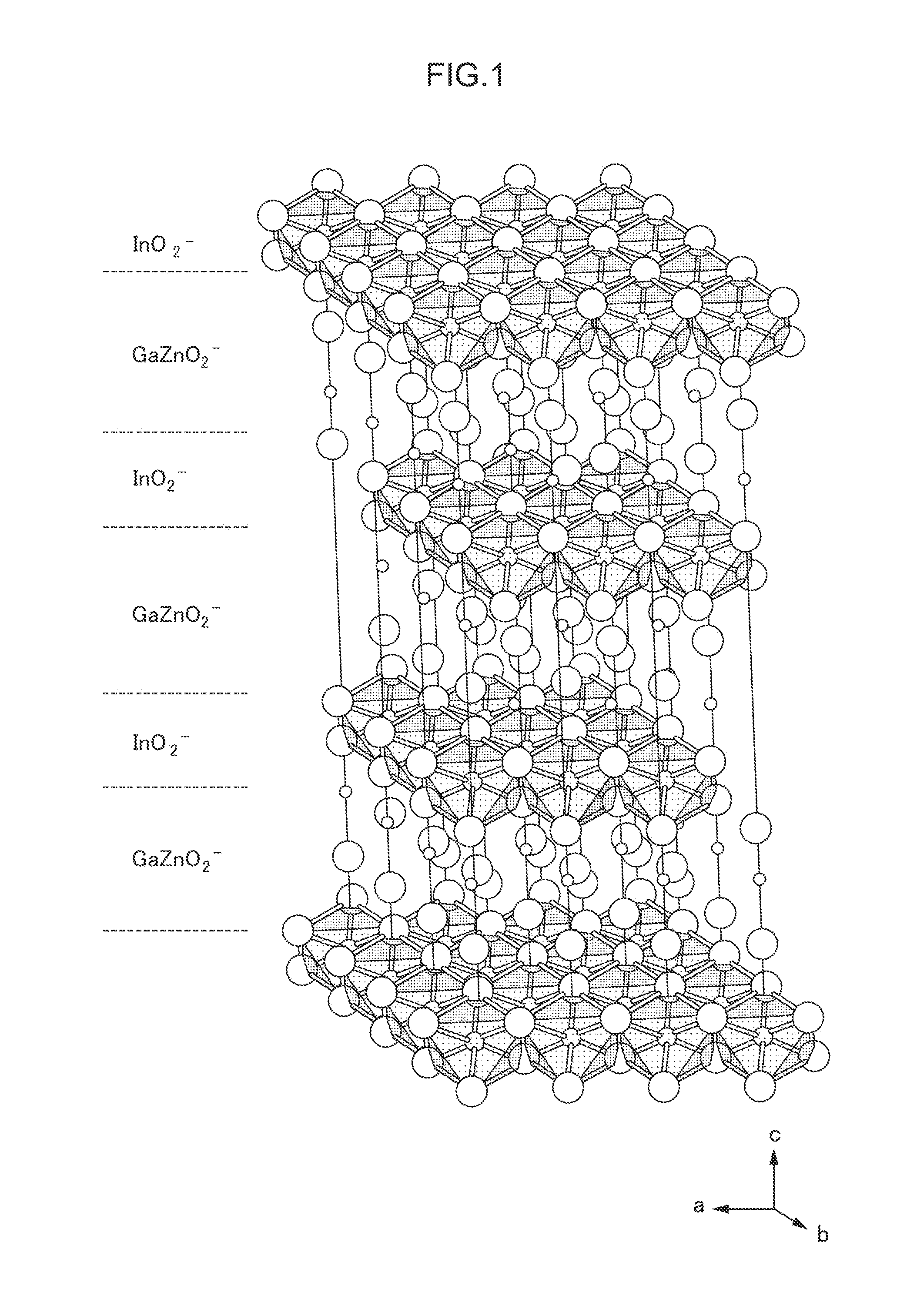
[0040]The IGZO-based oxide material according to the first exemplary embodiment of the invention has a crystal IGZO phase represented by a composition formula of In2-xGaxO3(ZnO)m in which m=1. Specifically, in consideration of oxygen deficit, the material is formed from an IGZO...
second exemplary embodiment
[0084]In the following, the method of producing the (field-effect) TFT and the method of producing the same according to the second exemplary embodiment of the invention are described with reference to the drawings.
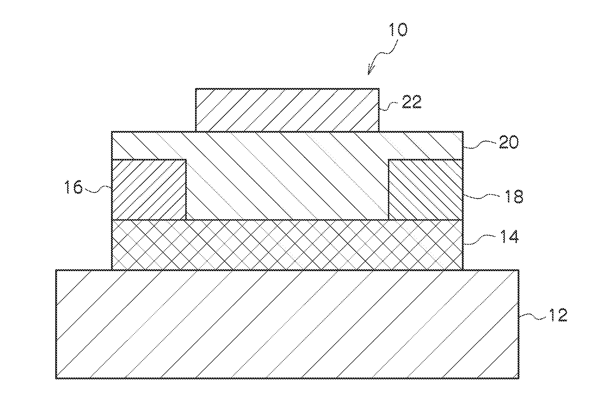
[0085]The TFT according to the second exemplary embodiment of the invention is an active device at least including a gate electrode, a gate insulating layer, an active layer, a source electrode and a drain electrode, and having a function of controlling an electric current that runs into the active layer by applying a voltage to the gate electrode, thereby switching the electric current that runs between the source electrode and the drain electrode.
[0086]The device structure of TFT may be inversely-staggered (also referred to as bottom-gate) or staggered (also referred to as top-gate), based on the position of gate electrode. Further, the TFT may have a top-contact structure or a bottom-contact structure, based on the position of a portion at which the active layer contac...
example 1
1. Preparation of Raw Materials
[0133]As the raw materials for the IGZO-based oxide material according to Example 1 of the invention, an oxide powder of In2O3 (manufactured by Kojundo Chemical Lab. Co., Ltd., purity: 99.99%), an oxide powder of Ga2O3 (manufactured by Kojundo Chemical Lab. Co., Ltd., purity: 99.99%), and an oxide powder of ZnO (manufactured by Kojundo Chemical Lab. Co., Ltd., purity: 99.99%) were prepared.
2. Measurement and Mixing of Raw Material Powders
[0134]These oxide powders were measured using an electronic balance such that the molar ratio of In:Ga:Zn is 2−x:x:1(0.5≦x≦1.2). For example, when the molar ratio of In:Ga:Zn is 1: 1:1 (x=1), the mass of In2O3 is 30.0000 g, the mass of Ga2O3 is 20.2430 g, and the mass of ZnO is 17.5758 g.
[0135]These oxide powders were placed in a polyethylene wide-month bottle together with 100 ml of ethyl alcohol and 150 alumina balls having a diameter of 10 mm. This wide-mouth bottle is sealed so that the liquid was not spilled out, ...
PUM
| Property | Measurement | Unit |
|---|---|---|
| resistivity | aaaaa | aaaaa |
| crystallization temperature | aaaaa | aaaaa |
| crystallization temperature | aaaaa | aaaaa |
Abstract
Description
Claims
Application Information