Method of and device for determining and controlling the distance between an integrated circuit and a substrate

Inactive Publication Date: 2010-12-23
NXP BV
View PDF13 Cites 0 Cited by
  • Summary
  • Abstract
  • Description
  • Claims
  • Application Information

AI Technical Summary

Benefits of technology

[0031]It is also possible to apply an auxiliary layer, particularly a transparent auxiliary layer, to the integrated circuit. The auxiliary layer may be applied to the entire integrated circuit or only partially. The auxiliary layer may help to reliably detect even a relative smal

Problems solved by technology

Since the parameters of the mounting process, e.g. heat, pressure, the properties of the integrated circuits, the substrate, the adhesive, etc. vary, the distance between the substrate and the integrated circuit is relatively hard to control.
Because several integrated circuits

Method used


Image

  • Method of and device for determining and controlling the distance between an integrated circuit and a substrate
  • Method of and device for determining and controlling the distance between an integrated circuit and a substrate
  • Method of and device for determining and controlling the distance between an integrated circuit and a substrate

Examples


Embodiment Construction

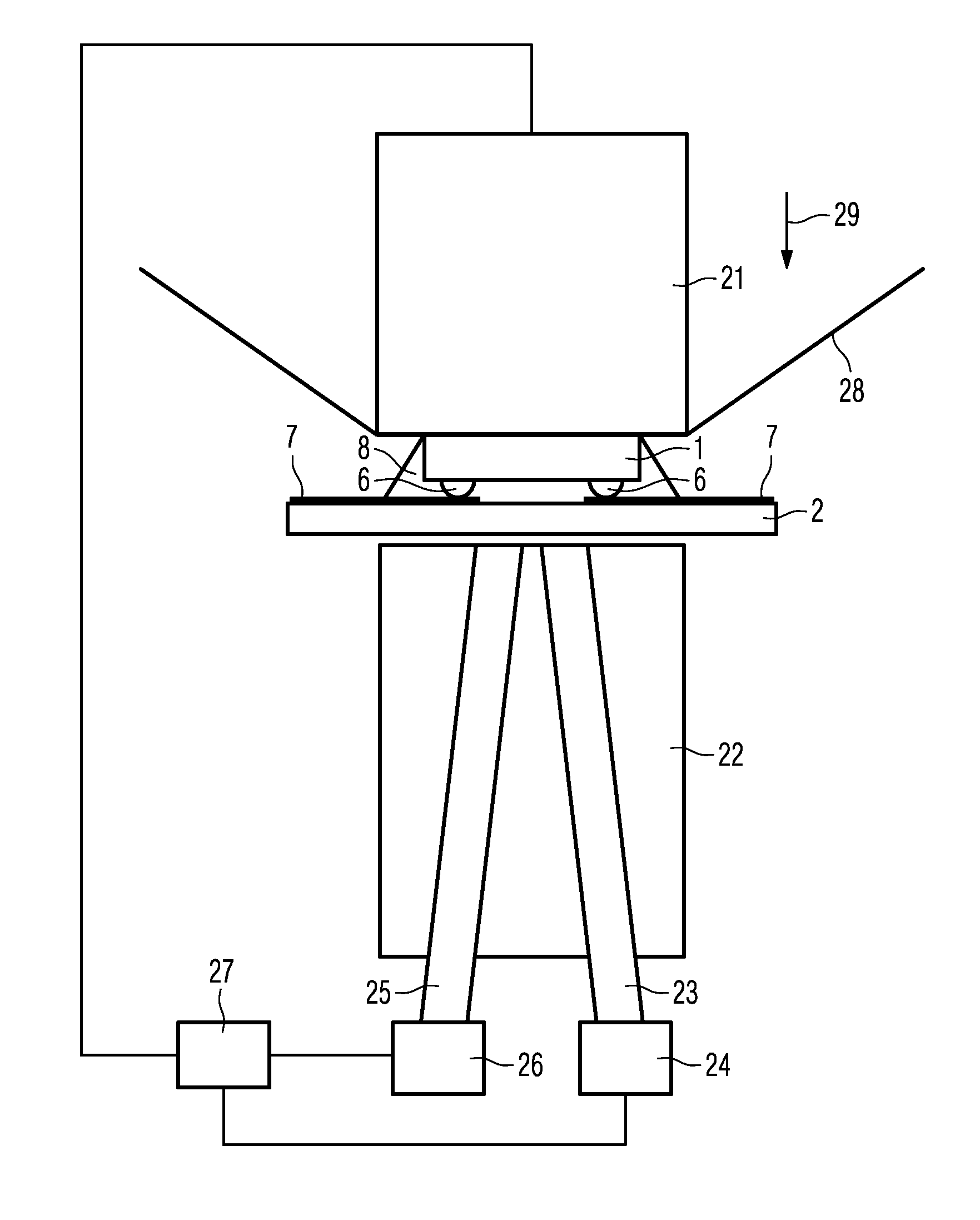
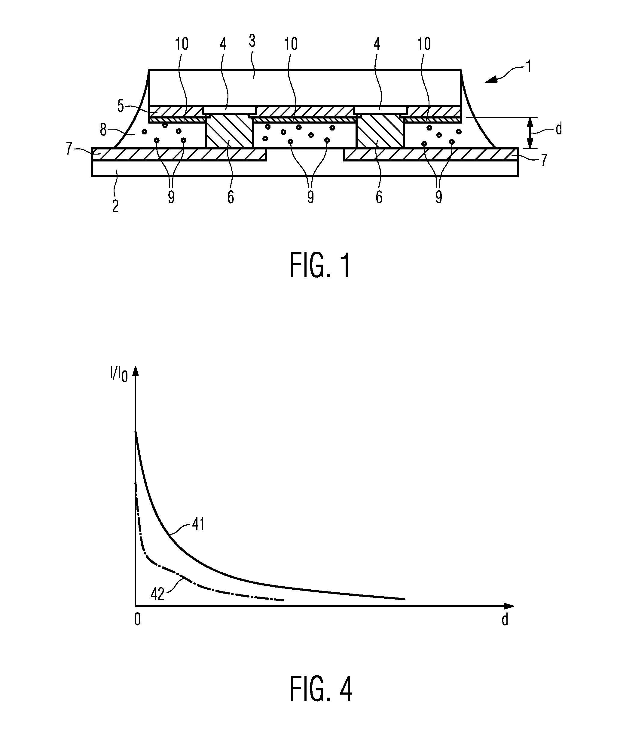
[0039]FIG. 1 shows an integrated circuit 1 attached to a substrate 2. The integrated circuit 1 may, for instance, be an integrated circuit for an RFID transponder and the substrate 2 may be a strap, via which contacts of the integrated circuits 1 are connected to an antenna of the RFID transponder.

[0040]According to the exemplary embodiment, the integrated circuit 1 comprises a main body 3 that includes the circuitry of the integrated circuit 1, connection pads 4, a passivation layer 5, and bumps 6. The substrate 2 comprises a metallization structure 7 applied on a first surface of the substrate 2. The metallization structure 7 may be made from aluminum and form contacts, for instance, to connect the bumps 6 to the antenna.

[0041]The passivation layer 5 is a sealing layer to prevent the circuitry from deterioration of the electric properties through chemical reaction, corrosion, or handling during a packaging process. The material of the passivation layer 5 is silicon dioxide accordi...


PUM


Abstract

In a method of determining the distance (d) between an integrated circuit (1) and a substrate (2) emitted light enters the at least semi transparent substrate (2), passes through the substrate (2) and an at least semi transparent material (8), is reflected by the integrated circuit (1), passes again through the material (8) and the substrate (2), and leaves the substrate (2). The at least semi transparent material (8), particularly is an at least semi transparent adhesive, provided between the substrate (2) and the integrated circuit (1). The distance (d) between the substrate (2) and the integrated circuit (1) is determined by evaluating the intensities of the light leaving and entering the substrate (2), particularly by evaluating the ratio between the intensities of the light leaving and entering the substrate (2).

Description

FIELD OF THE INVENTION[0001]The invention relates to a method of and a device for determining the distance between an integrated circuit and a substrate. Furthermore, the invention relates to a method of and a device for controlling attaching an integrated circuit to a substrate.BACKGROUND OF THE INVENTION[0002]Flip chip technology for manufacturing electronic devices is well known in prior art. Here an integrated circuit, which is also referred to as a chip, is mounted on a substrate such that connecting bumps of the integrated circuit electrically contact contacts of the substrate. In order to accomplish contact between the bumps and the substrate contacts, the integrated circuit is pressed against the substrate and heated such that the bumps partly penetrate the substrate contacts and an adhesive between the substrate and the integrated circuit cures. The tool used for pressing the integrated circuit to the substrate and applying heat is usually referred to as a thermode.[0003]Si...

Claims


Application Information

Patent Timeline
IPC IPC(8): H01L21/66G01B11/06
CPCG01B11/0625
Inventor ZENZ, CHRISTIAN
Owner NXP BV
Why Eureka
Try Eureka