
Liquid crystal display device and method of manufacturing the same

a liquid crystal display and liquid crystal technology, applied in the field of lcd devices and manufacturing methods, can solve the problems of uneven pretilt angles of liquid crystal molecules, rm injection between first and second substrates may not be easily cured at the surface of alignment layers, etc., to achieve the effect of improving afterimages and reliability

Active Publication Date: 2011-02-03
TCL CHINA STAR OPTOELECTRONICS TECH CO LTD
View PDF15 Cites 38 Cited by
  • Summary
  • Abstract
  • Description
  • Claims
  • Application Information

AI Technical Summary

Benefits of technology

[0009]Exemplary embodiments of the invention provide a liquid crystal display (“LCD”) device having improved afterimages and reliability.
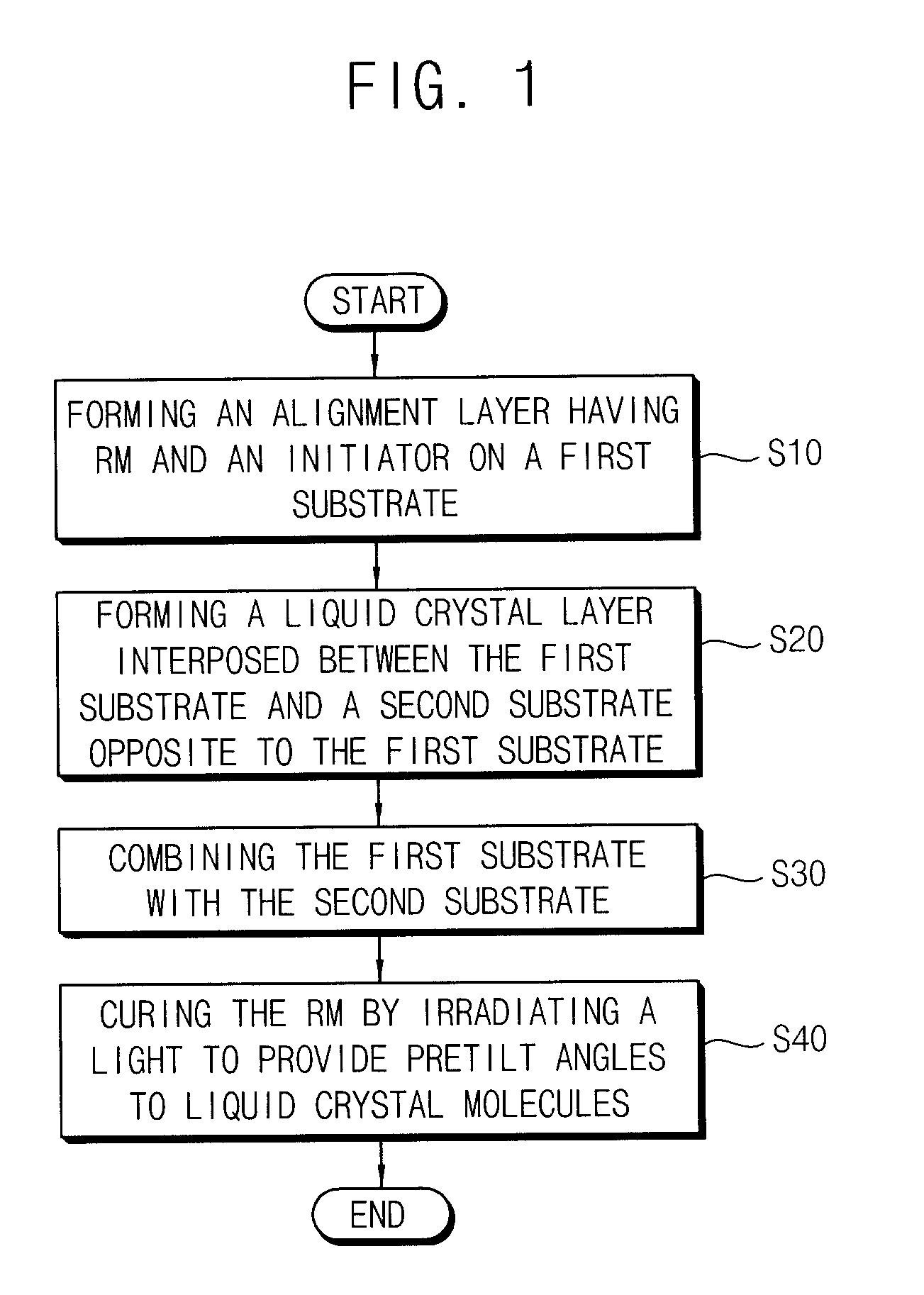
[0028]According to the invention, a reactive mesogen (“RM”) and an initiator are mixed with an alignment layer, not a liquid crystal. Thus, reliability deterioration by elution of remaining RM may be decreased, so that display quality may be improved.

Problems solved by technology

However, the RM injected between first and second substrates may not be easily cured at a surface of the alignment layer, and the RM may remain in the liquid crystal layer.
Thus, pretilt angles of liquid crystal molecules may not be uniform.

Method used


Image

  • Liquid crystal display device and method of manufacturing the same
  • Liquid crystal display device and method of manufacturing the same
  • Liquid crystal display device and method of manufacturing the same

Examples


Embodiment Construction

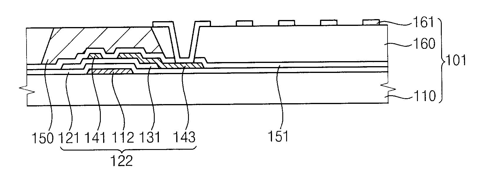
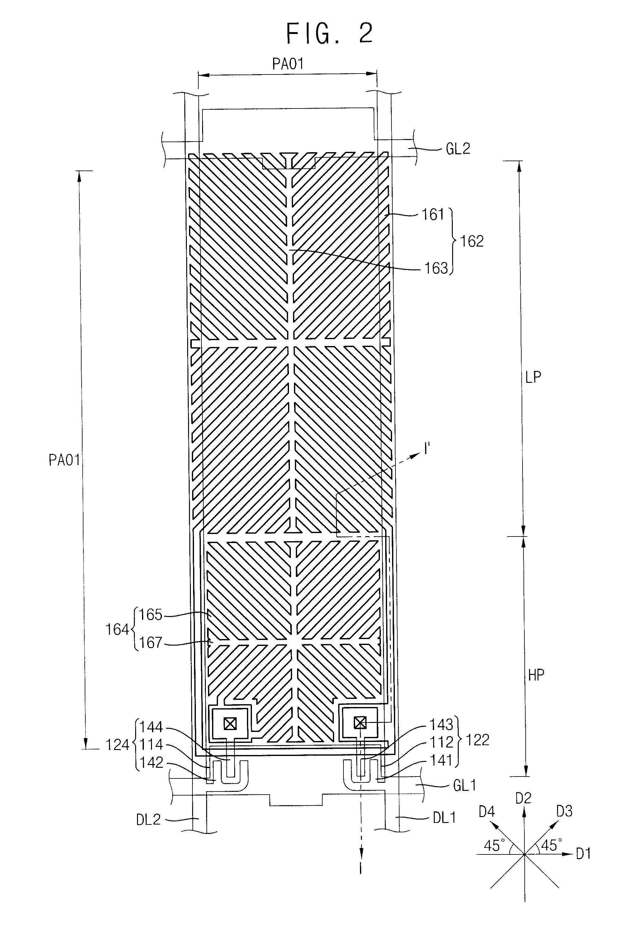
[0037]The invention is described more fully hereinafter with reference to the accompanying drawings, in which exemplary embodiments of the invention are shown. The invention may, however, be embodied in many different forms and should not be construed as limited to the exemplary embodiments set forth herein. Rather, these exemplary embodiments are provided so that this disclosure will be thorough and complete, and will fully convey the scope of the invention to those skilled in the art. In the drawings, the sizes and relative sizes of layers and regions may be exaggerated for clarity.

[0038]It will be understood that when an element or layer is referred to as being “on” or “connected to” another element or layer, it can be directly on or connected to the other element or layer or intervening elements or layers may be present. In contrast, when an element is referred to as being “directly on” or “directly connected to” another element or layer, there are no intervening elements or lay...


PUM

PropertyMeasurementUnit
pretilt anglesaaaaaaaaaa
total weightaaaaaaaaaa
electric fieldaaaaaaaaaa

Abstract

In a method of forming a liquid crystal display device, a black matrix is disposed on a substrate including a switching element formed thereon, a color filter is disposed on the switching element, a pixel electrode is electrically connected to the switching element, and a first alignment layer is disposed on the pixel electrode, to form a first substrate. A second substrate including a second alignment layer is formed. At least one of the first alignment layer and the second alignment layer includes a reactive mesogen. A liquid crystal layer is interposed between the first substrate and the second substrate. A light is irradiated onto the second substrate to provide pretilt angles of liquid crystal molecules of the liquid crystal layer.

Description

[0001]This application claims priority to Korean Patent Application No. 2009-69001, filed on Jul. 28, 2009, and all the benefits accruing therefrom under 35 U.S.C. §119, the contents of which are herein incorporated by reference in their entirety.BACKGROUND OF THE INVENTION[0002]1. Field of the Invention[0003]Exemplary embodiments of the invention relate to a liquid crystal display (“LCD”) device, and a method of manufacturing the LCD device. More particularly, exemplary embodiments of the invention relate to a liquid crystal display (“LCD”) device capable of enhancing afterimages and reliability, and a method of manufacturing the LCD device.[0004]2. Description of the Related Art[0005]Generally, in a liquid crystal display (“LCD”) device, a voltage is applied to an electric field generating electrode to provide the liquid crystal layer with an electric field, and arrangement of liquid crystal molecules of a liquid crystal layer is controlled in response to the electric field, there...

Claims


Application Information

Patent Timeline
Patent Type & Authority Applications(United States)
IPC IPC(8): G02F1/1337B05D3/06
CPCG02F1/133711G02F2001/133726G02F1/133788G02F1/133726G02F1/133753G02F1/136209G02F1/133715G02F1/134345G02F1/136222
Inventor SOHN, JI-WONYEOM, JOO-SEOKHEO, JEONG-UKBYUN, HO-YUNLEE, JUNG-HUNSHIN, NA-YOUNG
Owner TCL CHINA STAR OPTOELECTRONICS TECH CO LTD
Learn More