Electrically Interconnected Stacked Die Assemblies

a technology of stacked dies and interconnections, applied in the direction of electrical equipment, semiconductor devices, semiconductor/solid-state device details, etc., can solve problems such as electrical shorting in the wire loop

Active Publication Date: 2011-02-17
INVENSAS CORP
View PDF99 Cites 73 Cited by
  • Summary
  • Abstract
  • Description
  • Claims
  • Application Information

AI Technical Summary

Benefits of technology

Openings in the electrical insulation expose at least selected die pads or interconnect terminals. The openings may in some embodiments be made following formation of the insulation. For example where the electrical insulation includes a conformal coating, such as a parylene, openings may be

Problems solved by technology

If the vertical clearance is insufficient, overlying features may interfere with or introduce electrical short

Method used


Image

  • Electrically Interconnected Stacked Die Assemblies
  • Electrically Interconnected Stacked Die Assemblies
  • Electrically Interconnected Stacked Die Assemblies

Examples


Embodiment Construction

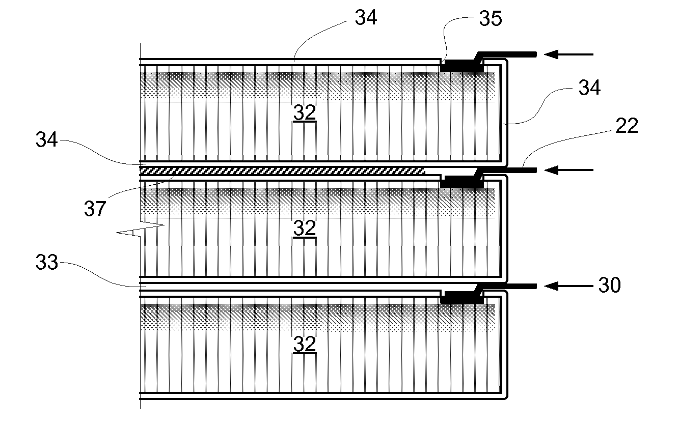
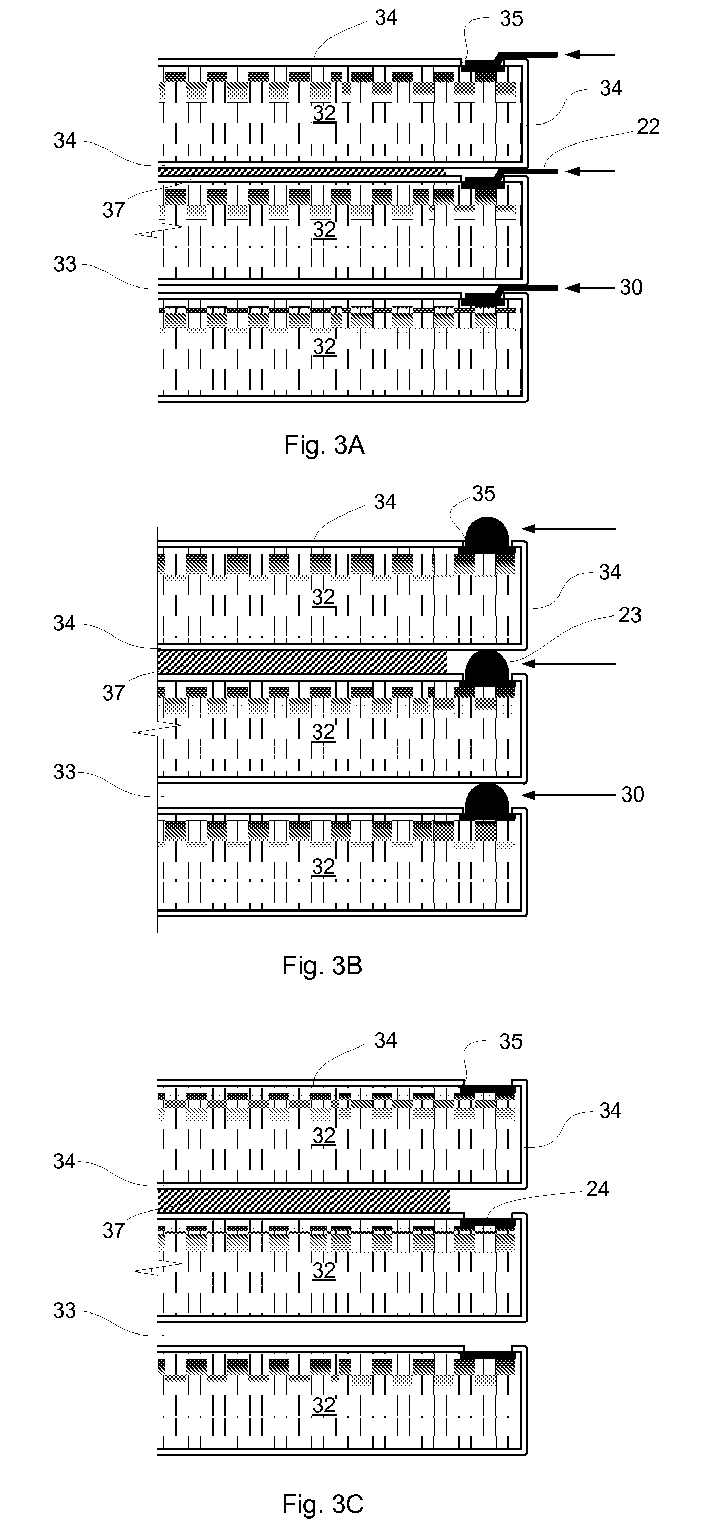
The invention will now be described in further detail by reference to the drawings, which illustrate alternative embodiments of the invention. The drawings are diagrammatic, showing features of the invention and their relation to other features and structures, and are not made to scale. For improved clarity of presentation, in the FIGS. illustrating embodiments of the invention, elements corresponding to elements shown in other drawings are not all particularly renumbered, although they are all readily identifiable in all the FIGS. Also for clarity of presentation certain features are not shown in the FIGS., where not necessary for an understanding of the invention.

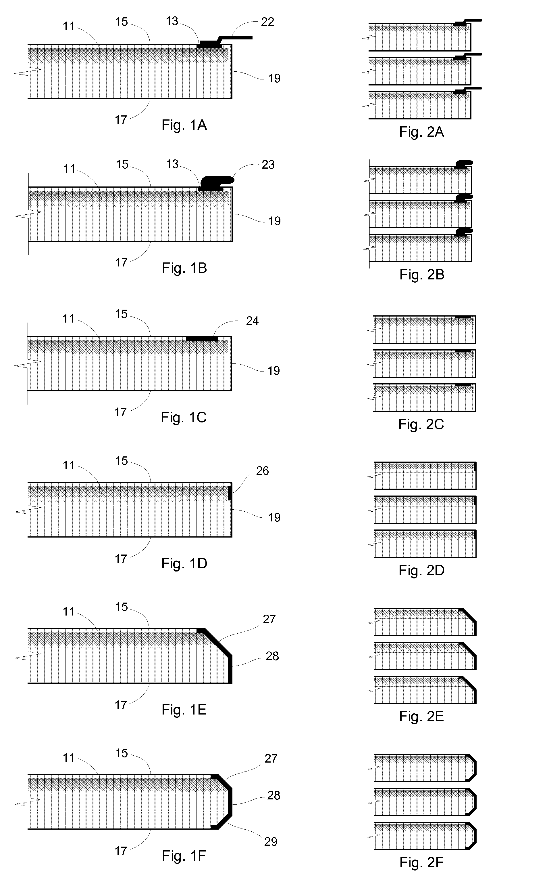
FIGS. 1A-1F show examples of various die edge configurations in die to be interconnected according to various embodiments of the invention.

FIG. 1A shows a die having an “off-die” interconnect. The die is shown in a partial sectional view, having an active side 15 at which the integrated circuitry 11 of the die is formed, ...


PUM


Abstract

In die stack assembly configurations successive die in the stack are offset at a die edge at which die pads are situated, and the die are interconnected by electrically conductive traces. In some embodiments the electrically conductive traces are formed of an electrically conductive polymer. An electrically insulative conformal coating is provided having openings at die pads that are electrically connected.

Description

BACKGROUNDThis invention relates to electrical interconnection of integrated circuit chips and, particularly, to interconnection of stacked die.A typical semiconductor die has a front (“active”) side, in which the integrated circuitry is formed, a back side, and sidewalls. The sidewalls meet the front side at front edges and the back side at back edges. Semiconductor die typically are provided with interconnect pads (die pads) located at the front side for electrical interconnection of the circuitry on the die with other circuitry in the device in which the die is deployed. Some die as provided have die pads on the front side along one or more of the die margins, and these may be referred to as peripheral pad die. Other die as provided have die pads arranged in one or two rows at the front side near the center of the die, and these may be referred to as central pad die. The die may be “rerouted” to provide a suitable arrangement of interconnect pads at or near one or more of the mar...

Claims


Application Information

Patent Timeline
IPC IPC(8): H01L23/52
CPCH01L24/24H01L2224/82102H01L24/82H01L25/0657H01L25/50H01L2224/24011H01L2224/24145H01L2224/24226H01L2224/48091H01L2224/48095H01L2224/48145H01L2224/48465H01L2224/76155H01L2225/06524H01L2225/06551H01L2225/06555H01L2225/06562H01L2924/01013H01L2924/01015H01L2924/01038H01L2924/01074H01L2924/01078H01L2924/01079H01L2924/01082H01L2924/14H01L24/25H01L2224/32145H01L2924/014H01L2924/01047H01L2924/01033H01L2924/01006H01L2924/01005H01L2924/00014H01L2924/00H01L2924/00012
Inventor MCELREA, SIMON J. S.ANDREWS, JR., LAWRENCE DOUGLASMCGRATH, SCOTTCASKEY, TERRENCECRANE, SCOTT JAYROBINSON, MARC E.CANTILLEP, LORETO
Owner INVENSAS CORP
Why Eureka
Try Eureka