Pixel array and driving method thereof and flat panel display

a technology of pixel array and driving method, which is applied in the direction of electric digital data processing, instruments, computing, etc., can solve the problems of charge rate becomes an important issue, and bright/dark line display defect is generated, so as to achieve the effect of removing bright/dark line display d

Inactive Publication Date: 2011-03-17
AU OPTRONICS CORP
View PDF5 Cites 21 Cited by
  • Summary
  • Abstract
  • Description
  • Claims
  • Application Information

AI Technical Summary

Benefits of technology

[0008]The present invention is directed to a pixel array and a driving method thereof, and a flat panel display using the driving method, so as to mitigate a display defect of bright / dark lines.

Problems solved by technology

Therefore, a charge rate becomes an important issue.
For example, at a tail end of the data line, a data line delay can lead to different charge rates of odd sub-pixels and even sub-pixels, so that a display defect of bright / dark lines is generated.
Moreover, at a tail end of the scan line, a scan line delay leads to a result that a gate is not disabled during a polarity conversion, so that the defect of the bright / dark lines is generated due to a charge error of the even sub-pixels.

Method used


Image

  • Pixel array and driving method thereof and flat panel display
  • Pixel array and driving method thereof and flat panel display
  • Pixel array and driving method thereof and flat panel display

Examples


first embodiment

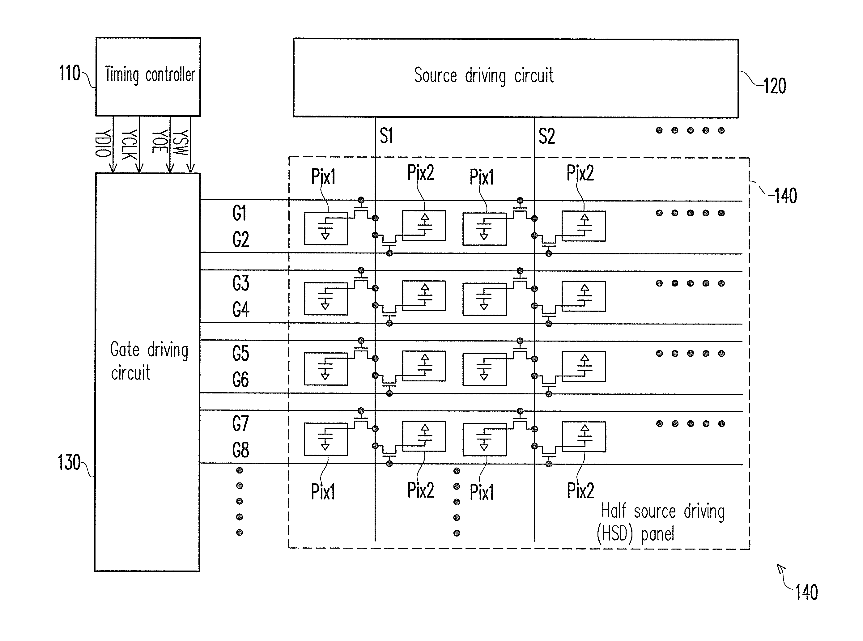
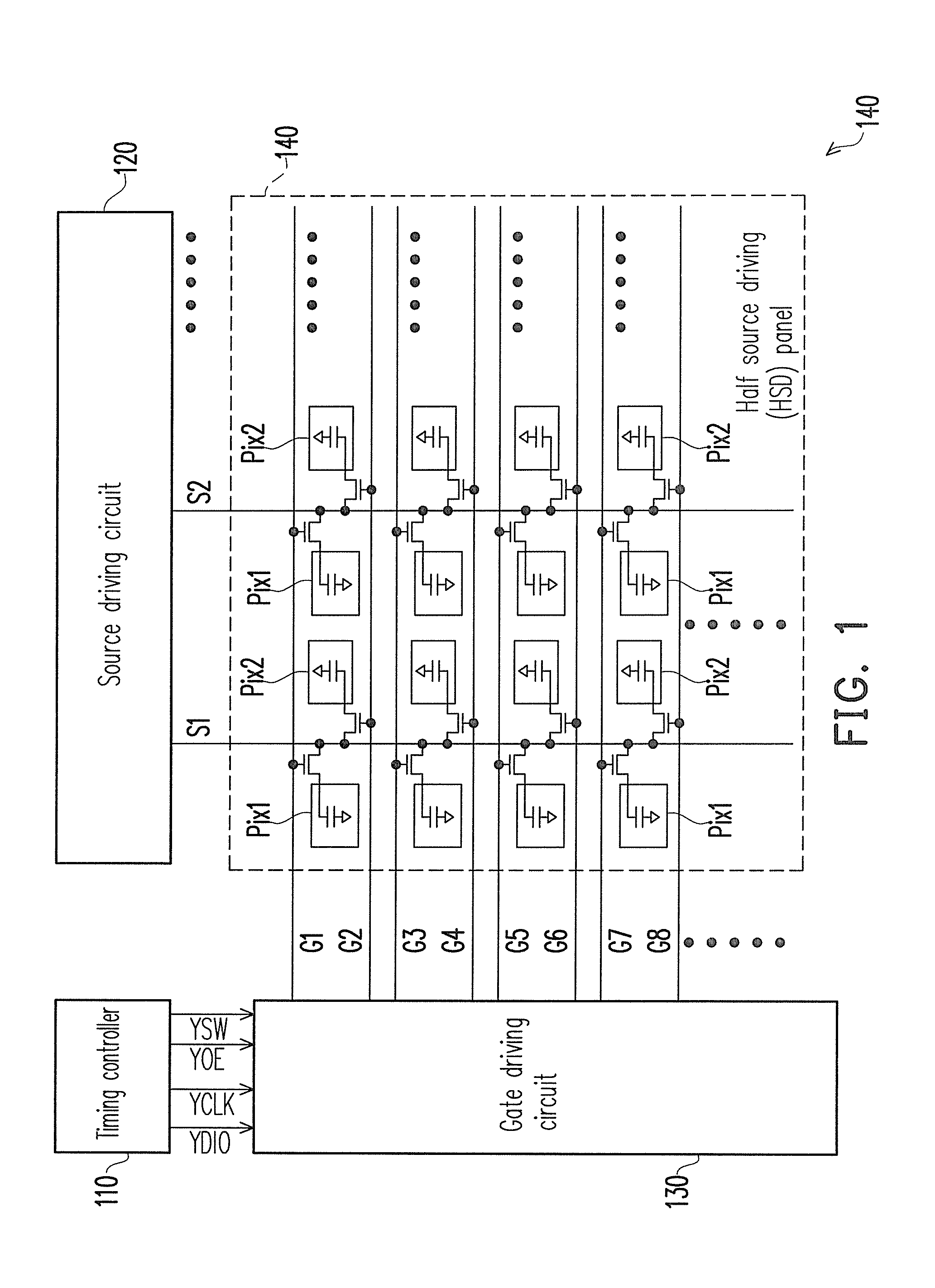
[0030]In the present embodiment, a (2n+1)-th frame is regarded as the aforementioned first frame period, and a (2n+2)-th frame is regarded as the aforementioned second frame period, wherein n is an integer. Moreover, in the present embodiment, a (2 m+1)-th pixel row on the HSD panel 140 is regarded as the aforementioned a-th pixel row, and a (2 m+2)-th pixel row is regarded as the aforementioned b-th pixel row, wherein m is an integer.

[0031]FIG. 3 is a timing diagram of signal waveforms of FIG. 1 according to an embodiment of the present invention. Referring to FIG. 1 and FIG. 3, in the (2n+1)-th frame (for example, a frame Frame1 or a frame Frame3 in FIG. 3), the gate driving circuit 130 provides a gate driving signal to the scan lines on the HSD panel 140 in a sequence of “the first scan line G1, the second scan line G2, the fourth scan line G4, the third scan line G3, . . . ”. Namely, the gate driving circuit 130 provides the gate driving signal to the scan lines on the HSD panel...

second embodiment

[0032]Similar to the first embodiment, the (2n+1)-th frame is regarded as the aforementioned first frame period, and the (2n+2)-th frame is regarded as the aforementioned second frame period. A difference between the present embodiment and the first embodiment is that a (4 m+1)-th pixel row on the HSD panel 140 is regarded as the aforementioned a-th pixel row, and a (4 m+3)-th pixel row is regarded as the aforementioned b-th pixel row. In the (2n+1)-th frame period, the (4 m+1)-th pixel row and the (4 m+2)-th pixel row on the HSD panel 140 are driven in a sequence of “the first scan line, the second scan line”, and the (4 m+3)-th pixel row and the (4 m+4)-th pixel row on the HSD panel 140 are driven in a sequence of “the second scan line, the first scan line”. In the (2n+2)-th frame period, the gate driving circuit 130 drives the (4 m+1)-th pixel row and the (4 m+2)-th pixel row in a sequence of “the second scan line, the first scan line”, and drives the (4 m+3)-th pixel row and the...

third embodiment

[0034]Similar to the first embodiment, the (2n+1)-th frame is regarded as the aforementioned first frame period, and the (2n+2)-th frame is regarded as the aforementioned second frame period. A difference between the present embodiment and the first embodiment is that six pixel rows (i.e. 12 scan lines) are taken as a cycle. In the first frame period, the gate driving circuit 130 drives a (6 m+1)-th pixel row, a (6 m+2)-th pixel row and a (6m+5)-th pixel row on the HSD panel 140 in a sequence of “the first scan line, the second scan line”, and drives a (6m+3)-th pixel row, a (6m+4)-th pixel row and a (6m+6)-th pixel row on the HSD panel 140 in a sequence of “the second scan line, the first scan line”. In the (2n+2)-th frame period, the gate driving circuit 130 drives the (6m+1)-th pixel row, the (6m+2)-th pixel row and the (6m+5)-th pixel row in a sequence of “the second scan line, the first scan line”, and drives the (6m+3)-th pixel row, the (6m+4)-th pixel row and the (6m+6)-th pi...


PUM


Abstract

A pixel array, a driving method thereof and a flat panel display using the same are provided. The pixel array includes a first, a second, a third, and a fourth scan lines. A plurality of pixels is disposed between the first and the second scan lines. A plurality of pixels is disposed between the third and the fourth scan lines. In a first frame period, a gate driving circuit sequentially provides a driving signal to the first, the second, the fourth and the third scan lines. In a second frame period, the gate driving circuit sequentially provides the driving signal to the second, the first, the third and the fourth scan lines.

Description

CROSS-REFERENCE TO RELATED APPLICATION[0001]This application claims the priority benefit of Taiwan application serial no. 98130910, filed Sep. 14, 2009. The entirety of the above-mentioned patent application is hereby incorporated by reference herein and made a part of specification.BACKGROUND OF THE INVENTION[0002]1. Field of the Invention[0003]The present invention relates to a flat panel display. More particularly, the present invention relates to a half source driving (HSD) panel pixel array and a driving method thereof.[0004]2. Description of Related Art[0005]Along with development of large-scale display panels, in various pixel array structures of current liquid crystal display (LCD) panels, there is a so-called half source driving (HSD) structure. According to the HSD structure, a number of data lines can be reduced to a half, so that a price of a source driver is accordingly reduced. In detail, in a pixel array of the HSD structure, two adjacent sub-pixels share one data lin...

Claims


Application Information

Patent Timeline
Patent Type & Authority Applications(United States)
IPC IPC(8): G09G5/00
CPCG09G3/3648G09G3/3677G09G2320/0223G09G2300/0465G09G2310/0297G09G2300/0426
Inventor HSU, CHAO-CHINGLIN, WEI-CHENGTSAI, YU-CHUN
Owner AU OPTRONICS CORP
Why Eureka
Try Eureka