Method of manufacturing a display panel

a technology of display panel and manufacturing method, which is applied in the manufacture of electrode systems, electric discharge tubes/lamps, instruments, etc., can solve the problems of display panel thin film transistor damage, display panel damage, and polluted alignment members, so as to reduce the damage of display panel and reduce the effect of display panel

Inactive Publication Date: 2011-04-19
SAMSUNG DISPLAY CO LTD
View PDF6 Cites 7 Cited by
  • Summary
  • Abstract
  • Description
  • Claims
  • Application Information

AI Technical Summary

Benefits of technology

[0009]Embodiments of the present invention provide a method of manufacturing a display panel capable of preventing afterimages from being displayed.
[0015]According to the embodiments of the present invention, defects of a display panel may be reduced, and the display panel may be prevented from displaying afterimages.

Problems solved by technology

Particularly, liquid crystal display (LCD) devices are being rapidly developed according to demand since the LCD devices are thin and light weight, and consume low power.
However, the alignment member may be polluted by fine dust attached to the cloth and fibers of the cloth.
In addition, thin film transistors (TFTs) of the display panel may be damaged by static electricity caused by rubbing the surface of the alignment member.
However, when the alignment member is formed by the photo-alignment method, the display panel may display afterimages because the polar anchoring energy of the alignment member is small.

Method used


Image

  • Method of manufacturing a display panel
  • Method of manufacturing a display panel
  • Method of manufacturing a display panel

Examples


Embodiment Construction

[0024]The present invention is described more fully hereinafter with reference to the accompanying drawings, in which example embodiments of the present invention are shown. The present invention may, however, be embodied in many different forms and should not be construed as limited to the example embodiments set forth herein. In the drawings, the sizes and relative sizes of layers and regions may be exaggerated for clarity.

[0025]It will be understood that when an element or layer is referred to as being “on,”“connected to” or “coupled to” another element or layer, it can be directly on, connected or coupled to the other element or layer or intervening elements or layers may be present.

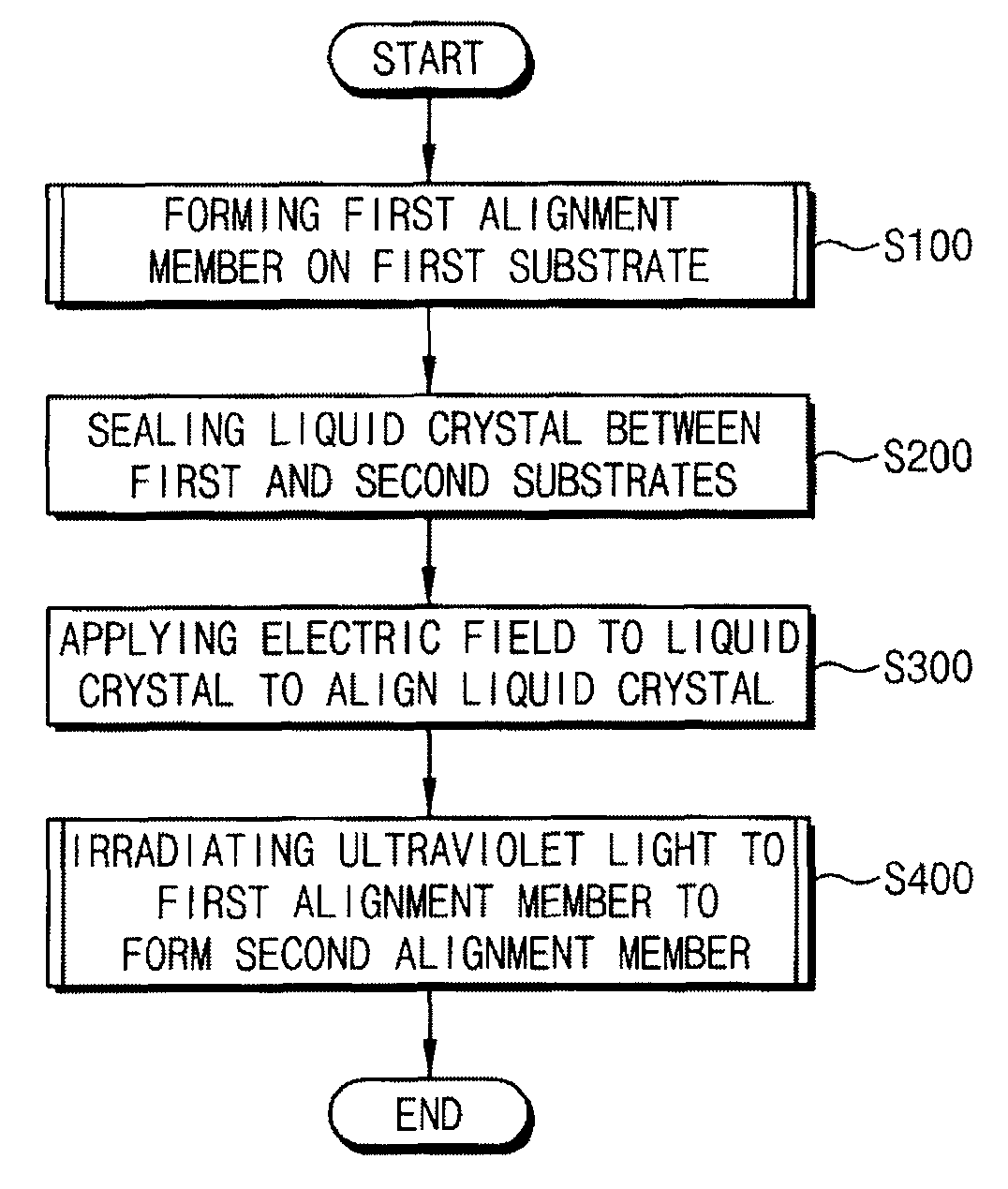
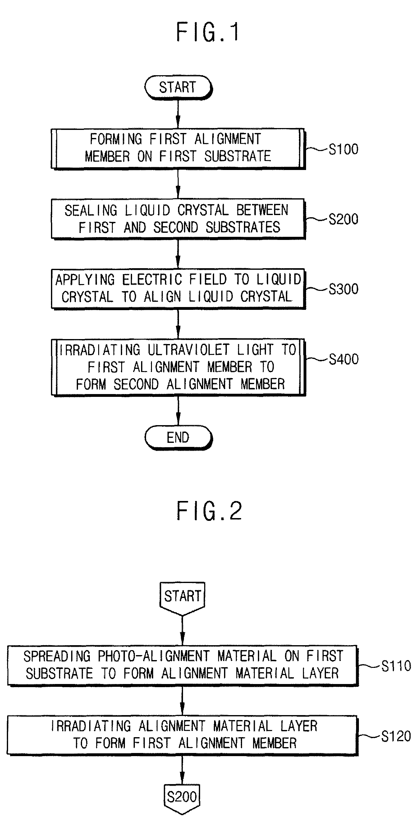
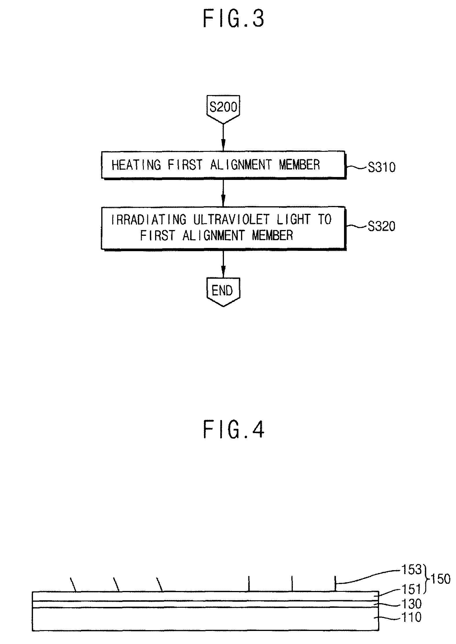
[0026]FIGS. 1 to 3 are flowcharts illustrating a method of manufacturing a display panel in accordance with an embodiment of the present invention.

[0027]Referring to FIGS. 1 to 3, a first alignment member is formed on a first substrate (step S100).

[0028]For example, an alignment material is spread on...


PUM

PropertyMeasurementUnit
electric fieldaaaaaaaaaa
voltageaaaaaaaaaa
temperatureaaaaaaaaaa

Abstract

In a method of manufacturing a display panel, a first alignment member is formed on a first substrate. Liquid crystal is sealed between the first substrate and a second substrate opposite to the first substrate. Then, an electric field is applied to the liquid crystal to align the liquid crystal. Ultraviolet light is irradiated onto the first alignment member to form a second alignment member while applying the electric field to the liquid crystal.

Description

CROSS-REFERENCE TO RELATED APPLICATIONS[0001]This application claims priority to Korean Patent Application No. 2008-9147, filed on Jan. 29, 2008 in the Korean Intellectual Property Office (KIPO), the contents of which are incorporated herein by reference in their entirety.BACKGROUND OF THE INVENTION[0002]1. Technical Field[0003]Embodiments of the present invention relate to a method of manufacturing a display panel. More particularly, embodiments of the present invention relate to a method of manufacturing a display panel capable of improving image quality.[0004]2. Discussion of the Related Art[0005]In the modern information age, display devices are being developed to process information and display images using the processed information. Particularly, liquid crystal display (LCD) devices are being rapidly developed according to demand since the LCD devices are thin and light weight, and consume low power.[0006]An LCD device displays images using the properties of liquid crystal mol...

Claims


Application Information

Patent Timeline
Patent Type & Authority Patents(United States)
IPC IPC(8): G02F1/1337
CPCG02F1/133788G02F2001/133757G02F1/133757G02F1/1337
Inventor SHIN, YONG-HWANLEE, JUN-WOO
Owner SAMSUNG DISPLAY CO LTD
Why Eureka
Try Eureka