Liquid crystal display device and method of driving a liquid crystal display device

a liquid crystal display and display device technology, applied in the field of display devices, can solve the problem of inconspicuous display unevenness

Inactive Publication Date: 2007-09-11
SEMICON ENERGY LAB CO LTD +1
View PDF13 Cites 64 Cited by
  • Summary
  • Abstract
  • Description
  • Claims
  • Application Information

AI Technical Summary

Benefits of technology

[0033]Through the above structure and method, vertical streaks are prevented from being displayed on the screen even when analog buffer circuits built on an insulating substrate are fluctuated in output.

Problems solved by technology

Consequently, output fluctuation among the analog buffer circuits is time-averaged, and display unevenness is thus made inconspicuous.

Method used


Image

  • Liquid crystal display device and method of driving a liquid crystal display device
  • Liquid crystal display device and method of driving a liquid crystal display device
  • Liquid crystal display device and method of driving a liquid crystal display device

Examples


embodiment 1

[Embodiment 1]

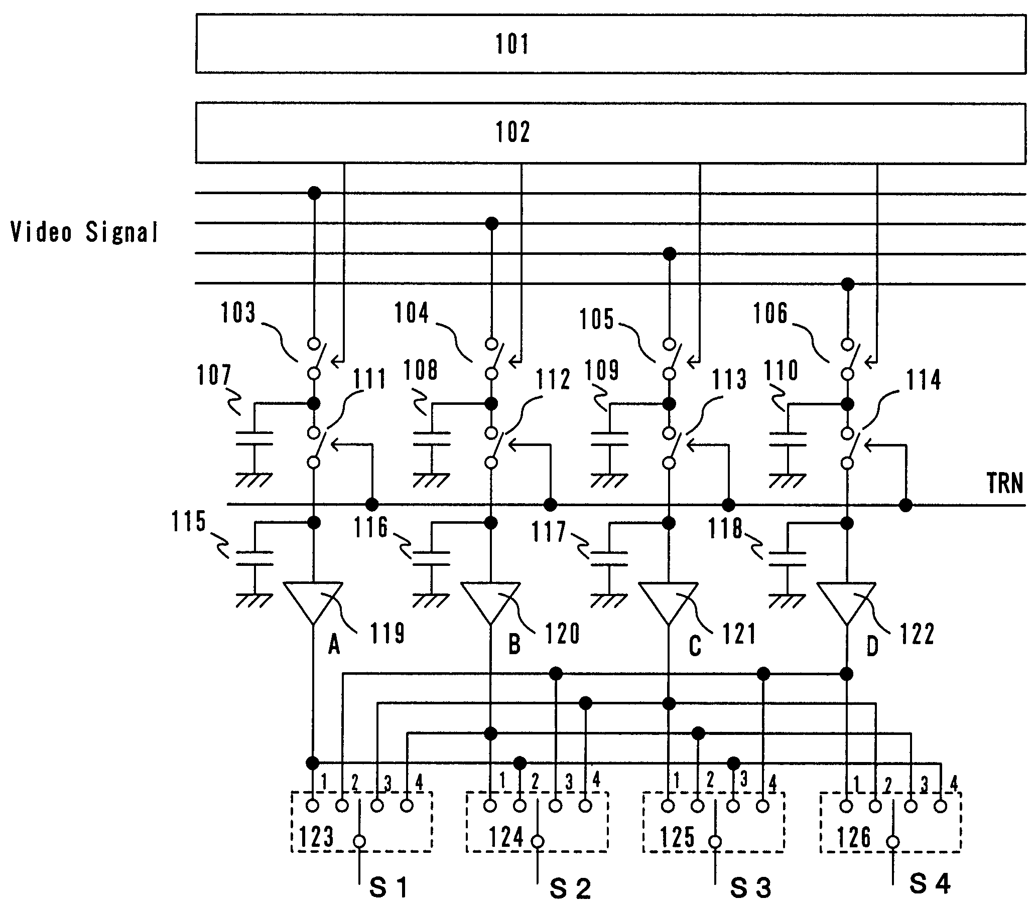
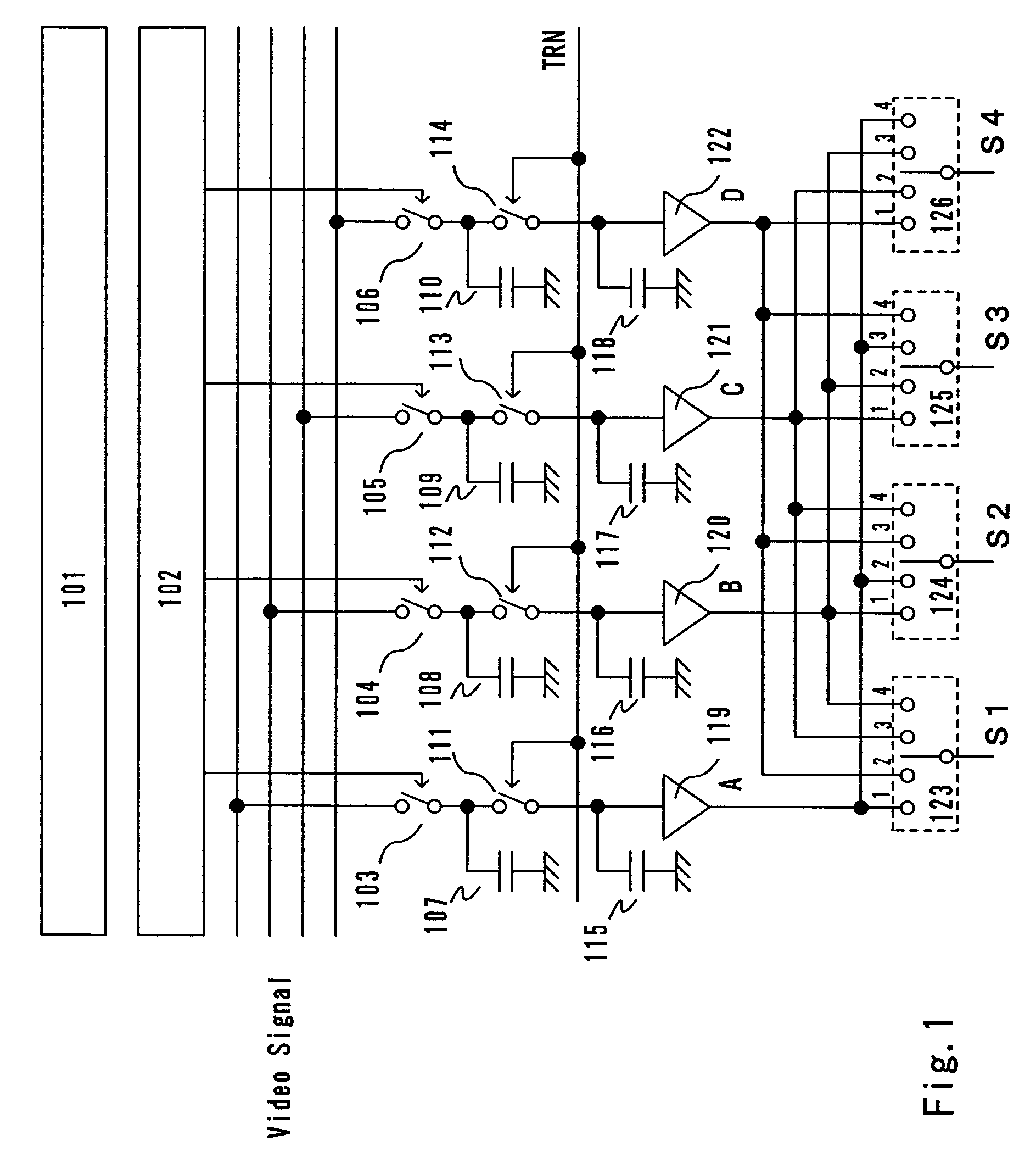
[0062]FIG. 7 shows Embodiment 1, which is a specific circuit example of the switch 123 of a switching means shown in FIG. 1. In this embodiment, analog switch circuits are used as the switching means. The switch is composed of TFTs 701 to 708 and is controlled by control lines 1, 1b, 2, 2b, . . . , and 4b, which are separately connected to gate terminals of the TFTs 701 to 708. FIG. 8 is a timing chart of the control lines 1 to 4b. Control signals shown in FIG. 8 connect A shown in FIG. 1, in FIG. 7 to source signal lines S1 to S4 during the first to fourth frame. The circuit diagram shown in FIG. 7 has a CMOS structure but may have an NMOS structure or a PMOS structure instead. In this case, the number of control lines is cut in half

embodiment 2

[Embodiment 2]

[0063]FIG. 5 shows an operation amplifier circuit as an example of an analog buffer circuit. The output voltage fluctuation of this type of analog buffer circuit depends on fluctuation in characteristic between TFTs 503 and 504, which constitute a differential circuit, and fluctuation between TFTs 501 and 502, which constitute a current mirror circuit. If fluctuation between adjacent TFTs in a pair is small, the overall fluctuation of the panel can be large without causing a problem. For that reason, operation amplifier type analog buffer circuits are often used in integrated circuits.

[0064]In this example, the differential circuit is composed of n-channel TFTs and the current mirror circuit is composed of p-channel TFTs. However, the present invention is not limited thereto and the polarities of these circuits may be reversed. Also, the present invention is not limited to the circuit connection shown in this example and any circuit connection can be employed as long a...

embodiment 3

[Embodiment 3]

[0065]FIG. 6 shows a source follower circuit as an example of an analog buffer circuit. The source follower circuit is composed of a buffer TFT 601 and a constant current source 602. In this example, the buffer TFT is an n-channel TFT but may be a p-channel TFT instead. When an n-channel TFT is used, the output electric potential of the source follower circuit is lower than the input electric potential by Vgs of the TFT. On the other hand, when a p-channel TFT is used, the output electric potential of the source follower circuit is higher than the input electric potential by Vgs of the TFT. Although the source follower circuit has this problem, it also has an advantage of having a simpler structure than CMOS. In the case where a unipolar process is employed in order to reduce the number of steps in manufacturing a TFT, it is difficult to build an operation amplifier type analog buffer circuit and therefore a source follower type is chosen.


PUM

PropertyMeasurementUnit
capacitanceaaaaaaaaaa
voltagesaaaaaaaaaa
voltagesaaaaaaaaaa

Abstract

A liquid crystal display device having analog buffer circuits, which is reduced in luminance fluctuation is provided. A source signal line driver circuit has a plurality of analog buffer circuits, the plurality of source signal lines and the plurality of analog buffer circuits constitute a circuit group, and source signal lines connected to the analog buffer circuits are switched their connections to different analog buffer circuits each time a new period is started. Therefore, output fluctuation among the analog buffer circuits is averaged and a uniform image can be displayed on the screen.

Description

BACKGROUND OF THE INVENTION[0001]1. Field of the Invention[0002]The present invention relates to a display device, and more particularly to an liquid crystal display device using thin film transistors (TFTs) formed over a transparent substrate made of glass, plastic, or the like and a driving method thereof. In addition, the present invention relates to electronic equipment using a liquid crystal display device.[0003]2. Description of the Related Art[0004]In recent years, mobile telephones have become widespread due to development of communication technology. In future, moving picture transmission and a larger amount of information transfer are further expected. With respect to a personal computer, products for mobile applications are manufactured due to a reduction in weight thereof. A large number of information terminals called PDAs starting with electronic notebooks are also manufactured and becoming widespread. In addition, with the development of display devices and the like, ...

Claims


Application Information

Patent Timeline
Patent Type & Authority Patents(United States)
IPC IPC(8): G09G3/36G02F1/133G09G3/20
CPCG09G3/3648G09G3/3677G09G3/3688G09G2300/0408G09G2310/0297G09G2320/0233G09G3/36
Inventor KOYAMA, JUNSHIONOIRI, YUTAKAMIYAKE, HIROYUKIHIRAYAMA, YASUHIROLEE, BUYEOL
Owner SEMICON ENERGY LAB CO LTD
Why Eureka
Try Eureka