Light emitting device and method for manufacturing the same

a technology of light emitting devices and manufacturing methods, which is applied in the direction of discharge tubes/lamp details, organic semiconductor devices, discharge tubes luminescnet screens, etc., can solve the problems of reducing the light-emitting efficiency of light-emitting elements, reducing the luminance of light-emitting elements, and shortened lifetimes of light-emitting elements, so as to achieve shorten the life, reduce the luminance of light-emitting elements, and high reliability

Active Publication Date: 2005-02-24
SEMICON ENERGY LAB CO LTD
View PDF6 Cites 68 Cited by
  • Summary
  • Abstract
  • Description
  • Claims
  • Application Information

AI Technical Summary

Benefits of technology

[0030] In the case of sealing an EL element for the top emission structure or the dual emission structure, the second sealing agent is cured by heating rather than by UV irradiation. Accordingly, the pixel portion is not damaged by the UV irradiation, and hence, the problems of decreasing luminance of the EL element and shortening lifetime thereof can be solved.
[0031] According to the invention as disclosed in the specification, in the sealing step of the top emission structure and the dual emission structure, the sealing agent covering the pixel portion can be cured without damaging the EL element due to UV irradiation even in the case of using a sealing device that only has a function of UV irradiation. As a result, a light emitting device with high reliability can be obtained.
[0032] Since the first sealing agent in the periphery of the pixel portion is cured at...

Problems solved by technology

Since the EL element is extremely and easily deteriorated by being oxidized or absorbing moisture due to existence of oxygen or moisture, there has been a problem that the light-emitting efficiency of the EL element is decreased...

Method used


Image

  • Light emitting device and method for manufacturing the same
  • Light emitting device and method for manufacturing the same
  • Light emitting device and method for manufacturing the same

Examples


embodiment

[0044] [Embodiment Mode 1]

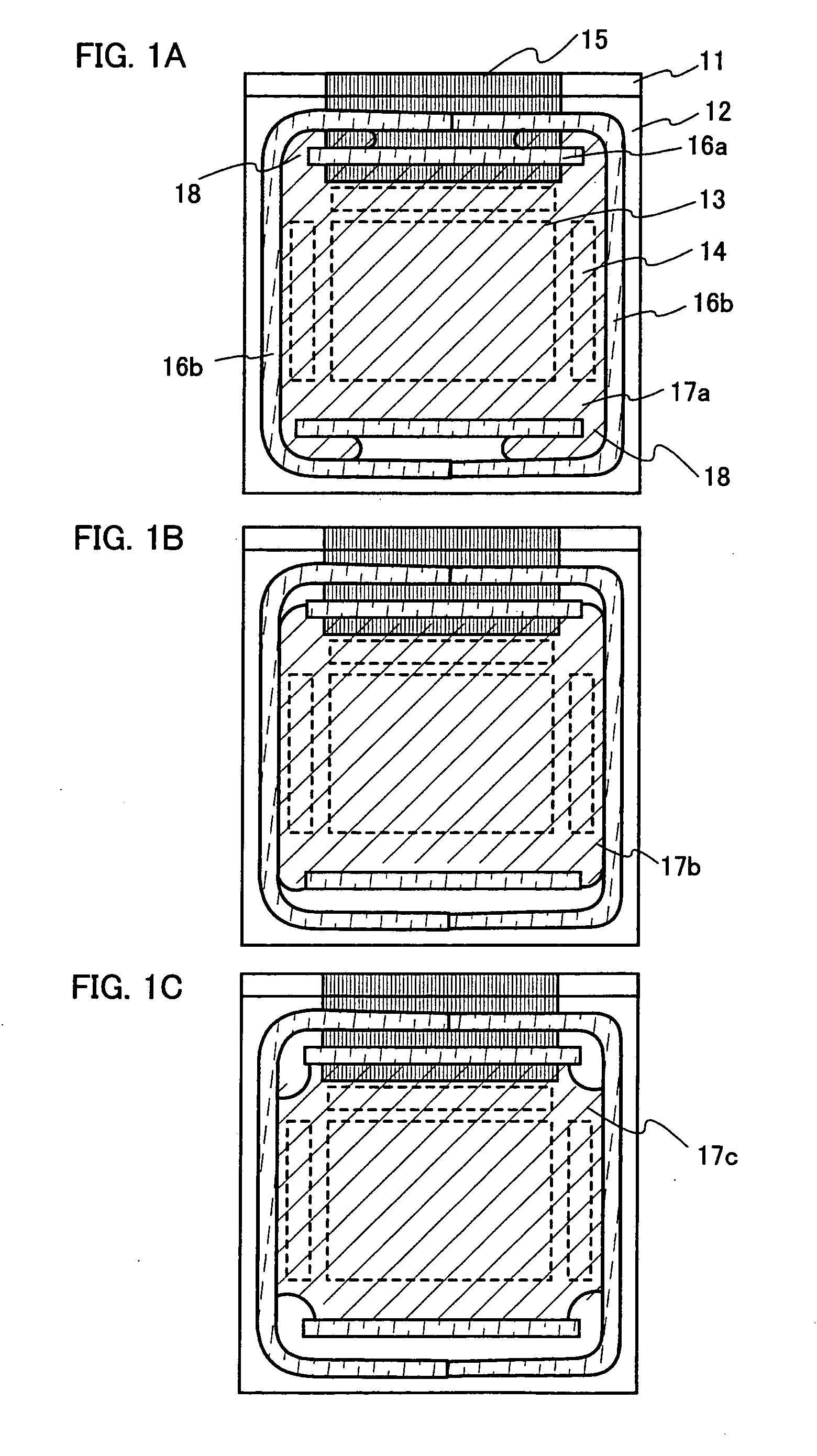
[0045]FIG. 1 is a top view of an active matrix light emitting device according to the present invention as disclosed in the specification.

[0046] In FIG. 1A, reference numeral 11 denotes a first substrate; 12, a second substrate; 13, a pixel portion; 14, a driver circuit portion; 15, a terminal portion; each of 16a and 16b; a first sealing agent; and 17a, a second sealing agent.

[0047] Though the material for the first substrate 11 is not particularly limited, the first substrate is preferably formed of a material having a same thermal expansion coefficient as that of the second substrate 12 from the viewpoint of attaching to the second substrate 12. In the case of the bottom emission structure, the first substrate 11 is formed of a substrate having a light transmitting property such as a glass substrate, a quartz substrate, and a plastic substrate. In the case of the top emission structure, a semiconductor substrate, a metal substrate, and the like can be ...

embodiment 1

[0090] [Embodiment 1]

[0091] An example of a light-emitting device comprising an EL element that uses a layer containing an organic compound as a light emitting layer will be described in the present embodiment with reference to FIG. 5.

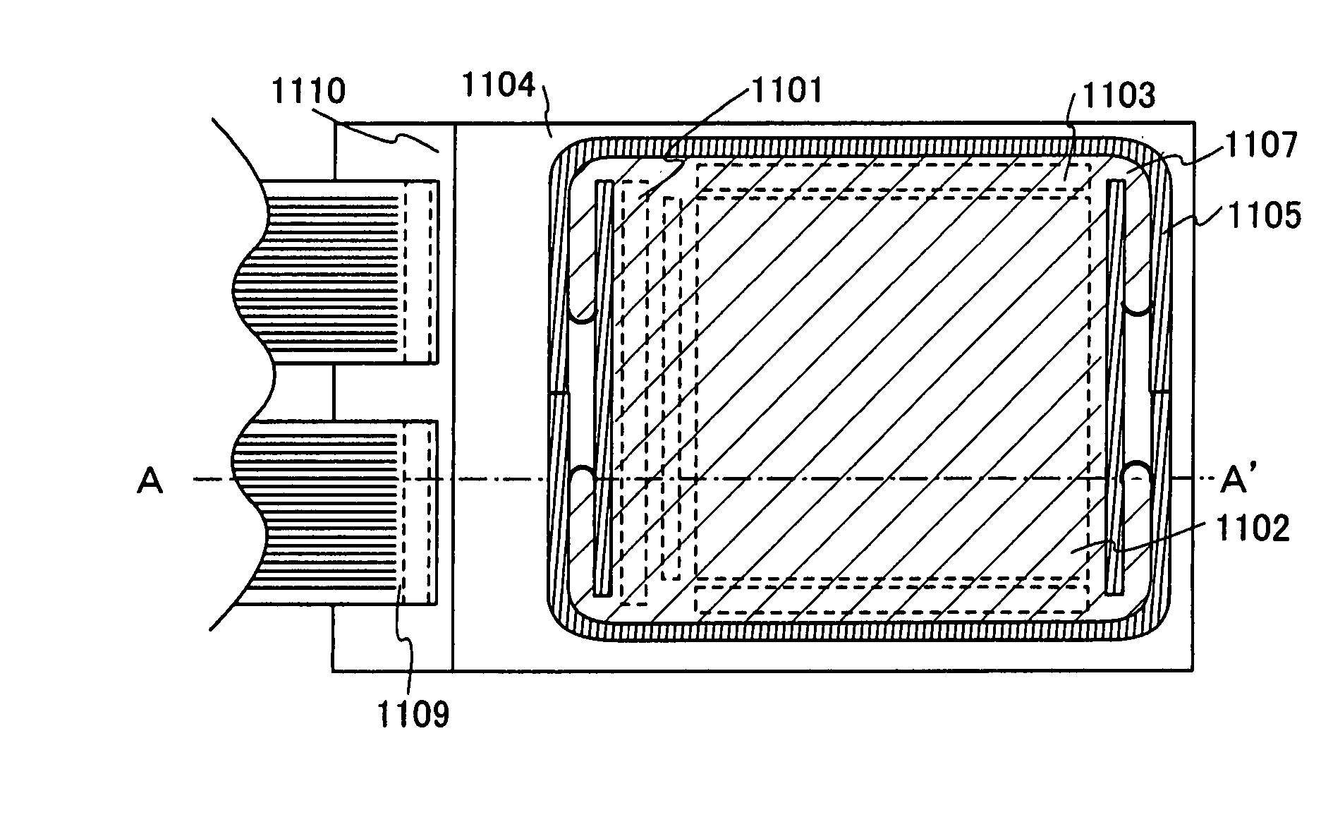
[0092]FIG. 5A is a top view of the light-emitting device and FIG. 5B is a cross-sectional view taken along a line A-A′ of FIG. 5A. Reference numeral 1101 denoted by a doted line is a source signal line driver circuit; 1102, a pixel portion; and 1103, a gate signal line driver circuit. Further, reference numeral 1104 denotes a sealing substrate and reference numeral 1105 denotes a first sealing agent. Inside surrounded by the first sealing agent 1105 is filled with a second transparent sealing agent 1107. Note that, the second sealing agent 1107 protrudes at four corners on a pixel region.

[0093] Reference numeral 1108 is a wiring for transmitting signals inputted to the source signal driver circuit 1101 and the gate signal line driver circuit 1103, an...

embodiment 2

[0104] [Embodiment 2]

[0105] In this embodiment, examples having different cross sectional structure from that of Embodiment Mode 2 will be shown in FIG. 6. In FIG. 6A, reference numeral 700 denotes a first substrate; each of 701a and 701b, an insulating layer; 702, a TFT; 709, an insulator; 710, an EL layer; 711, a second electrode; 712, a transparent protective layer; 713, a second sealing agent; and 714, a second substrate.

[0106] The TFT 702 (p-channel TFT) formed over the first substrate 700 is an element for controlling the electric current that flows through the EL layer 710 to emit light. Reference numeral 704 denotes a drain region (or a source region). Reference numeral 705 denotes a gate electrode. Though not shown in the drawings, one or a plurality of TFTs (n-channel TFTs or p-channel TFTs) is additionally provided for each pixel. Further, a TFT having one channel formation region 703 is illustrated here, but the present invention does not particularly limited thereto, a...


PUM


Abstract

When attaching a substrate with an EL element formed thereon and a transparent sealing substrate, the periphery of a pixel portion is surrounded with a first sealing agent that maintains a gap between the two pieces of substrates, an entire surface of the pixel portion is covered with a second transparent sealing agent so that the two pieces of substrate is fixed with the first sealing agent and the second sealing agent. Consequently, the EL element can be encapsulated by curing the first sealing agent and the second sealing agent without enclosing a drying agent and doing damage to the EL element due to UV irradiation even when a sealing device only having a function of UV irradiation is used.

Description

TECHNICAL FIELD [0001] The present invention as disclosed in the specification relates to a light emitting device having a light emitting layer which includes an organic compound, and a method for manufacturing the same. The present invention as disclosed in the specification further relates to an electronic appliance mounted with the light emitting device as a component. The light emitting device described in the present specification indicates, for example, an EL display device. BACKGROUND ART [0002] In recent years, research related to a light emitting device having an EL element as a self-luminous element has been actively carried out. Particularly, a light emitting device using an organic material as an EL material has been attracting attention. The light emitting device is also referred to as an EL display device. The EL element includes a layer containing an organic compound, which generates luminescence (electroluminescence) by being applied with an electric field (hereinaft...

Claims


Application Information

Patent Timeline
IPC IPC(8): H01L27/32H01L51/52H05B33/04
CPCH01L27/322H01L27/3244H01L51/5237H01L51/5256H01L2251/5315H01L2251/5323H05B33/04H01L51/5271H10K59/38H10K59/12H10K50/856H10K50/8426H10K2102/3026H10K2102/3031H10K50/846H10K50/8445H10K59/1213H10K71/00
Inventor KURIHARA, TOMOYUKI
Owner SEMICON ENERGY LAB CO LTD
Why Eureka
Try Eureka