
Apparatus for generating/detecting thz wave and method of manufacturing the same

a technology of terahertz wave and apparatus, which is applied in the direction of instruments, optical radiation measurement, spectrometry/spectrophotometry/monochromators, etc., can solve the problems of many limitations for development into portable measuring instruments, the fds-based apparatus for generating/detecting terahertz wave is still known as an expensive apparatus used only in laboratories, and the appropriate terahertz wave source technology meets the portable, non-cooling, and low-

Inactive Publication Date: 2011-03-24
ELECTRONICS & TELECOMM RES INST
View PDF12 Cites 16 Cited by
  • Summary
  • Abstract
  • Description
  • Claims
  • Application Information

AI Technical Summary

Benefits of technology

[0007]The present invention provides an apparatus for generating / detecting a Terahertz (THz) wave and a method of manufacturing the same, which can increase or maximize productivity by adopting cost-saving components and reducing difficulties of packaging technologies.
[0009]In some embodiments, the lens may be formed of a plastic material. Here, as the lens is formed of a cheap plastic material, the component price may be lowered. The plastic may have a refractive index of about 1.3 to about 1.5 in a terahertz wave range of 0.1 THz to 10 THz.
[0016]In even further embodiments, the first opening may have a smaller size than a diameter of the lens. The photo conductive layer exposed by the first opening may be supported by the bottom of the lens and may be prevented from being torn. The lens may be supported by a portion of the substrate at the outer edge of the first opening.
[0020]In even much further embodiment, the apparatus may further include an etch stopper layer on the entire undersurface of the photo conductive layer over the substrate. The etch stopper layer may protect the photo conductive layer in the forming of the first opening.
[0023]In other embodiments, the method may further include forming an etch stopper layer between the substrate and the photo conductive layer. The etch stopper layer may be formed between the substrate and the photo conductive layer to protect the photo conductive layer from an etchant or etching gas that etches the substrate in the forming of the first opening by the etching the substrate.

Problems solved by technology

Many studies are being conducted to develop a terahertz wave source operating in a frequency band of 0.1 THz to 10 THz, so-called terahertz gap, but have not yet been developed to an appropriate terahertz wave source technology meeting portable, non-cooling, and low-costing requirements necessary for commercialization.
Accordingly, there are many limitations for development into a portable measuring instrument due to high price and great system size.
However, since using various expensive components and delicate packaging technologies, this FDS-based apparatus for generating / detecting terahertz wave is still known as an expensive apparatus used only in laboratories.

Method used


Image

  • Apparatus for generating/detecting thz wave and method of manufacturing the same
  • Apparatus for generating/detecting thz wave and method of manufacturing the same
  • Apparatus for generating/detecting thz wave and method of manufacturing the same

Examples


first embodiment

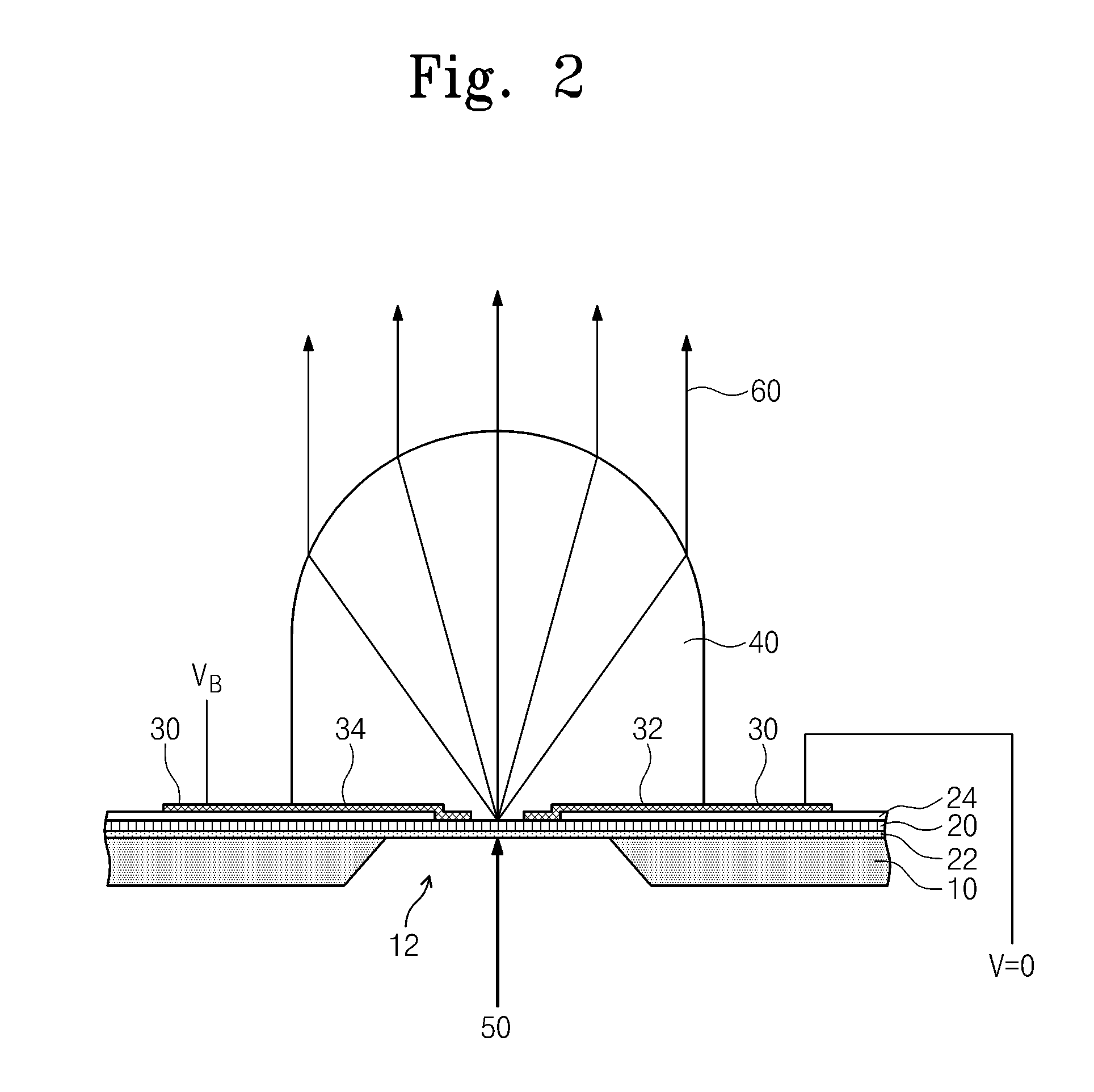
[0038]FIG. 2 is a cross-sectional view illustrating an apparatus for generating / detecting a Terahertz wave according to a

[0039]Referring to FIG. 2, an apparatus for generating / detecting a Terahertz wave according to a first embodiment includes an etch stopper layer 22 and a photo conductive layer 20 that are formed on a substrate 10 with a first opening 12, and first and second antenna electrodes 32 and 34 formed on the photo conductive layer 20 over the first opening 12 and spaced from each other by a certain gap. The apparatus for generating / detecting a Terahertz wave further includes a lens 40 filled in the gap between the first and second antenna electrodes 32 and 34 and protruding from the first and second antenna electrodes 32 and 34. The lens 40 contacts an exposed surface of the photo conductive layer 20 between the first and second antenna electrodes 32 and 34 and the surfaces of the first and second antenna electrodes 32 and 34. For example, the lens 40 may be strongly att...

second embodiment

[0057]FIG. 4 is a cross-sectional view illustrating an apparatus for generating / detecting a Terahertz wave according to a

[0058]Referring to FIG. 4, an apparatus for generating / detecting a Terahertz wave according to a second embodiment includes a photo conductive layer 20 and an insulating layer 44 that are stacked on a substrate 10 with a first opening 12, and first and second antenna electrodes 32 and 34 contacting the photo conductive layer 20 over the first opening 12 and spaced from each other by a certain gap. The apparatus for generating / detecting a Terahertz wave further includes a lens 40 formed on the photo conductive layer 20 exposed between the first and second antenna electrodes 32 and 34.

[0059]The lens 40 may be formed of plastic materials, and may be attached to the photo conductive layer 20 and the first and second antenna electrodes 32 and 34. The lens 40 may be attached to the substrate 10 as a component having various shapes such as spherical, oval, and cylindrica...


PUM


Abstract

Provided are an apparatus for generating / detecting terahertz wave and a method of manufacturing the same. The apparatus includes a substrate, a photo conductive layer, a first electrode and a second electrode, and a lens. The photo conductive layer is formed on an entire surface of the substrate. The first electrode and a second electrode are formed on the photo conductive layer. The first and second electrodes are spaced from each other by a certain gap. The lens is formed on the first and second electrodes. The lens is filled in the gap between the first and second electrodes.

Description

CROSS-REFERENCE TO RELATED APPLICATIONS[0001]This U.S. non-provisional patent application claims priority under 35 U.S.C. §119 of Korean Patent Application No. 10-2009-0088664, filed on Sep. 18, 2009, the entire contents of which are hereby incorporated by reference.BACKGROUND OF THE INVENTION[0002]The present invention disclosed herein relates to an apparatus for generating / detecting a Terahertz (THz) wave and a method of manufacturing the same, and more particularly, to an apparatus for generating / detecting a THz wave adopting a cost-saving lens and a method of manufacturing the same.[0003]A THz wave technology of 0.1 THz to 3 THz range in the electromagnetic band has a feature that transmits non-metallic and non-polar materials as well as a feature that resonant frequencies of very various molecules are distributed within the above range. The terahertz wave technology is a high-technology field that is expected to provide a new conceptual analysis technology that has never been i...

Claims


Application Information

Patent Timeline
IPC IPC(8): G01J5/00B44C1/22
CPCG01J3/10G01J3/42G01J5/0837H01S3/10
Inventor SHIN, JAEHEONPARK, KYUNG HYUNKIM, NAMJEHAN, SANG-PILLEE, CHUL-WOOKSIM, EUNDEOKBAEK, YONGSOON
Owner ELECTRONICS & TELECOMM RES INST
Learn More