Light emitting device with a coupled quantum well structure

a light-emitting device and quantum well technology, applied in the field of light-emitting devices with coupled quantum wells, can solve the problems of lowering the internal quantum efficiency (iqe), adversely affecting the reliability of the device, and creating extended defects such as misfit dislocations

Inactive Publication Date: 2011-05-05
RGT UNIV OF CALIFORNIA
View PDF3 Cites 25 Cited by
  • Summary
  • Abstract
  • Description
  • Claims
  • Application Information

AI Technical Summary

Benefits of technology

[0016]To overcome the limitations in the prior art described above, and to overcome other limitations that will become apparent upon reading and understanding the present specification, the present invention describes a coupled quantum well design in an active region of a light emitting device, wherein two or more wells are separated by one or more mini-barriers. By implementing a coupled quantum well structure, in a nonpolar (Al,Ga,In)N based light emitting device, for example, the problems described above may be alleviated, without affecting the quantum confinement to a large extent. A coupled quantum well structure provides almost the same effect as a wide quantum well, due to the coupling of the wavefunctions through the mini-barrier. The emission wavelength and the recombination efficiency can be tuned by varying the height and width of the mini-barrier.

Problems solved by technology

The problem with these structures, however, is that, due to the difference in material properties, for example, lattice mismatch, coefficient of thermal expansion (CTE) mismatch, etc., extended defects such as misfit dislocations are created at the well-barrier interface as a strain / stress relaxation mechanism.
The defects act as a non-radiative recombination center, resulting in a lowering of internal quantum efficiency (IQE) and adversely affecting device reliability.
Furthermore, it is difficult to grow thick InGaN wells of high In composition, required for green quantum wells, because of strain and InGaN segregation.
In c-plane devices, a single thick quantum is undesirable because of the enhanced quantum confined stark effect (QCSE) resulting in reduction of the overlap of electron and hole wavefunctions.

Method used


Image

  • Light emitting device with a coupled quantum well structure
  • Light emitting device with a coupled quantum well structure
  • Light emitting device with a coupled quantum well structure

Examples


Embodiment Construction

[0030]In the following description of the preferred embodiment, reference is made to the accompanying drawings which form a part hereof, and in which is shown by way of illustration a specific embodiment in which the invention may be practiced. It is to be understood that other embodiments may be utilized and structural changes may be made without departing from the scope of the present invention.

[0031]Device Structure and Fabrication Method

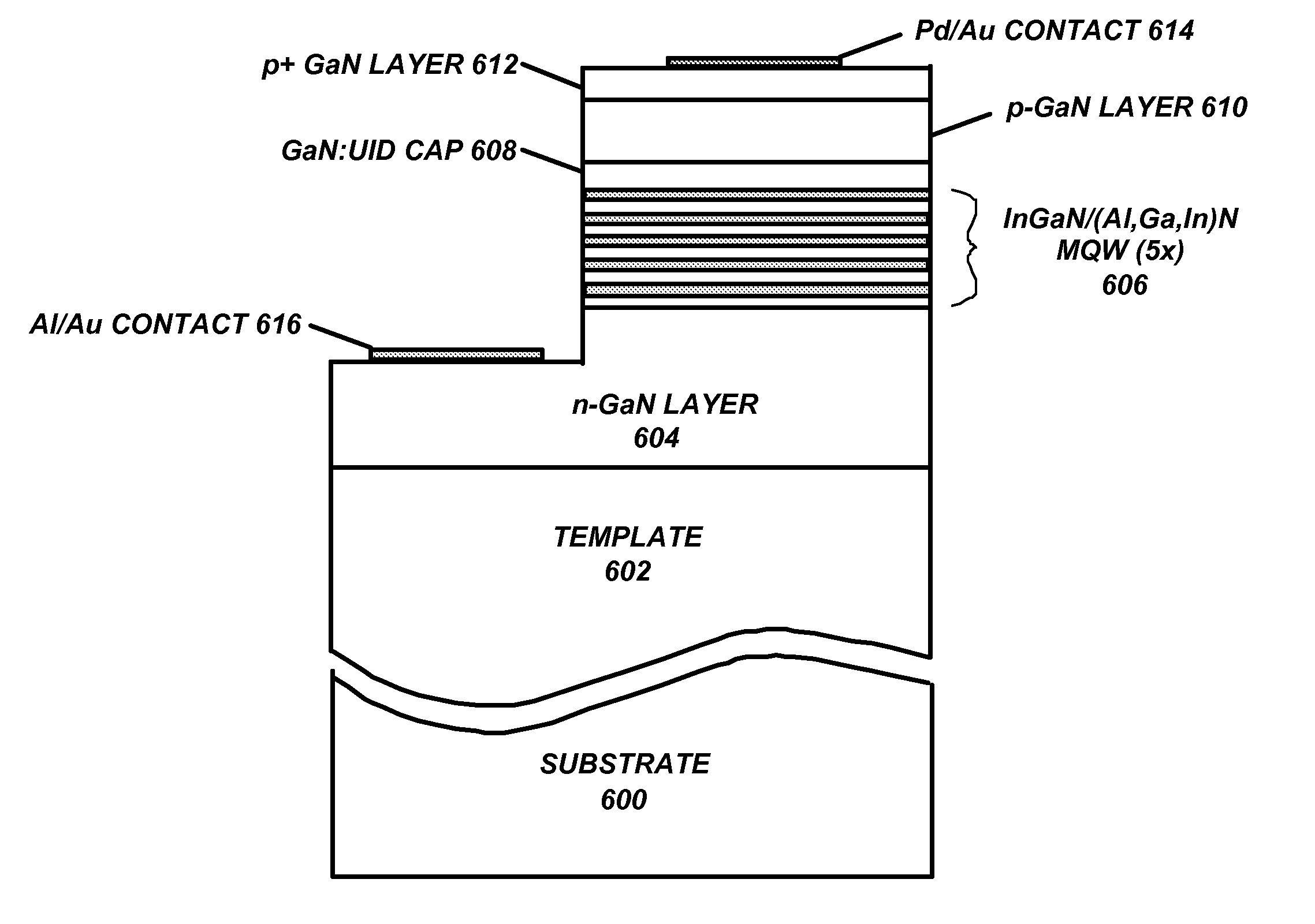
[0032]FIG. 5 is a flowchart describing the process steps for fabrication of a nonpolar, semipolar or polar (Al,Ga,In)N light emitting device according to the preferred embodiment of the present invention, while FIG. 6 is a schematic cross-section of a light emitting device fabricated in FIG. 5 according to the preferred embodiment of the present invention.

[0033]Block 500 represents the fabrication of a smooth, low-defect-density template on a substrate. For example, this Block may represent the fabrication, on an r-plane sapphire substrate 600, o...


PUM


Abstract

A light emitting device with a coupled quantum well structure in an active region. The coupled quantum well structure may include two or more wells are separated by one or more mini-barriers, and the wells and mini-barriers together are sandwiched by barriers. The coupled quantum well structure provides almost the same effect as a wide quantum well, due to the coupling of the wavefunctions through the mini-barrier. The light emitting device may be a nonpolar, semipolar or polar (Al,Ga,In)N based light emitting device.

Description

CROSS-REFERENCE TO RELATED APPLICATIONS[0001]This application claims the benefit under 35 U.S.C. Section 119(e) of co-pending and commonly assigned U.S. Provisional Patent Application Ser. No. 61 / 258,158, filed on Nov. 4, 2009, by You-Da Lin, Arpan Chakraborty, Shuji Nakamura, and Steven P. DenBaars, entitled “LIGHT EMITTING DEVICE WITH COUPLED QUANTUM WELLS,” attorney's docket number 30794.339-US-P1 (2010-274-1), which application is incorporated by reference herein.[0002]This application is related to co-pending and commonly-assigned U.S. Utility patent application Ser. No. 12 / 901,838, filed on Oct. 11, 2010, by Arpan Chakraborty, You-Da Lin, Shuji Nakamura, and Steven P. DenBaars, entitled “LIGHT EMITTING DEVICE WITH A STAIR QUANTUM WELL STRUCTURE” attorney's docket number 30794.321-US-U1 (2009-796-2), which application claims the benefit under 35 U.S.C. Section 119(e) of co-pending and commonly assigned U.S. Provisional Patent Application Ser. No. 61 / 250,391, filed on Oct. 9, 20...

Claims


Application Information

Patent Timeline
Patent Type & Authority Applications(United States)
IPC IPC(8): H01L33/06
CPCH01L33/32H01L33/06
Inventor LIN, YOU-DACHAKRABORTY, ARPANNAKAMURA, SHUJIDENBAARS, STEVEN P.
Owner RGT UNIV OF CALIFORNIA
Why Eureka
Try Eureka