Electroluminescent area illumination with integrated mechanical switch

a technology of electrically-luminescent area and control device, which is applied in the direction of lighting and heating apparatus, process and machine control, instruments, etc., can solve the problems of large and relatively expensive switch mechanism conventionally employed in lighting, wiring, and complex wiring circuits and sensors in buildings, etc., to achieve intelligent control, reduce manufacturing cost, and high level of integration

Active Publication Date: 2011-05-05
GLOBAL OLED TECH
View PDF12 Cites 11 Cited by
  • Summary
  • Abstract
  • Description
  • Claims
  • Application Information

AI Technical Summary

Benefits of technology

[0013]The present invention provides an improved control device for flat-panel, area-emissive lighting that includes a high level of integration at reduced manufacturing cost, intelligent control, and reduced infrastructure requirements.

Problems solved by technology

Such control methods for flat-panel area-emissive lighting are useful, but the switch mechanisms conventionally employed in lighting can be large and relatively expensive.
Techniques to do so can require an excessive number of external connections to the substrate, wiring to the lamp, and switches.
Moreover, the use of sensors and sophisticated control mechanisms to provide intelligent lighting can create complex and expensive wiring circuits and sensors in buildings that employ intelligent lighting control systems.

Method used


Image

  • Electroluminescent area illumination with integrated mechanical switch
  • Electroluminescent area illumination with integrated mechanical switch
  • Electroluminescent area illumination with integrated mechanical switch

Examples


Embodiment Construction

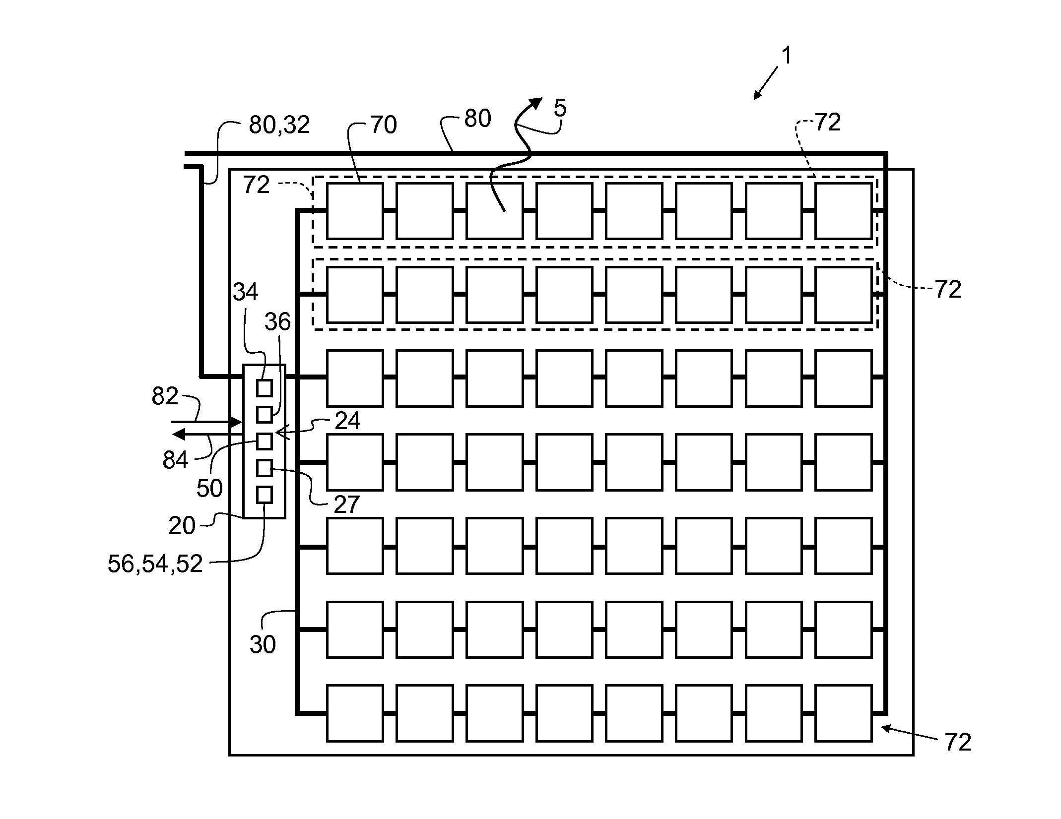
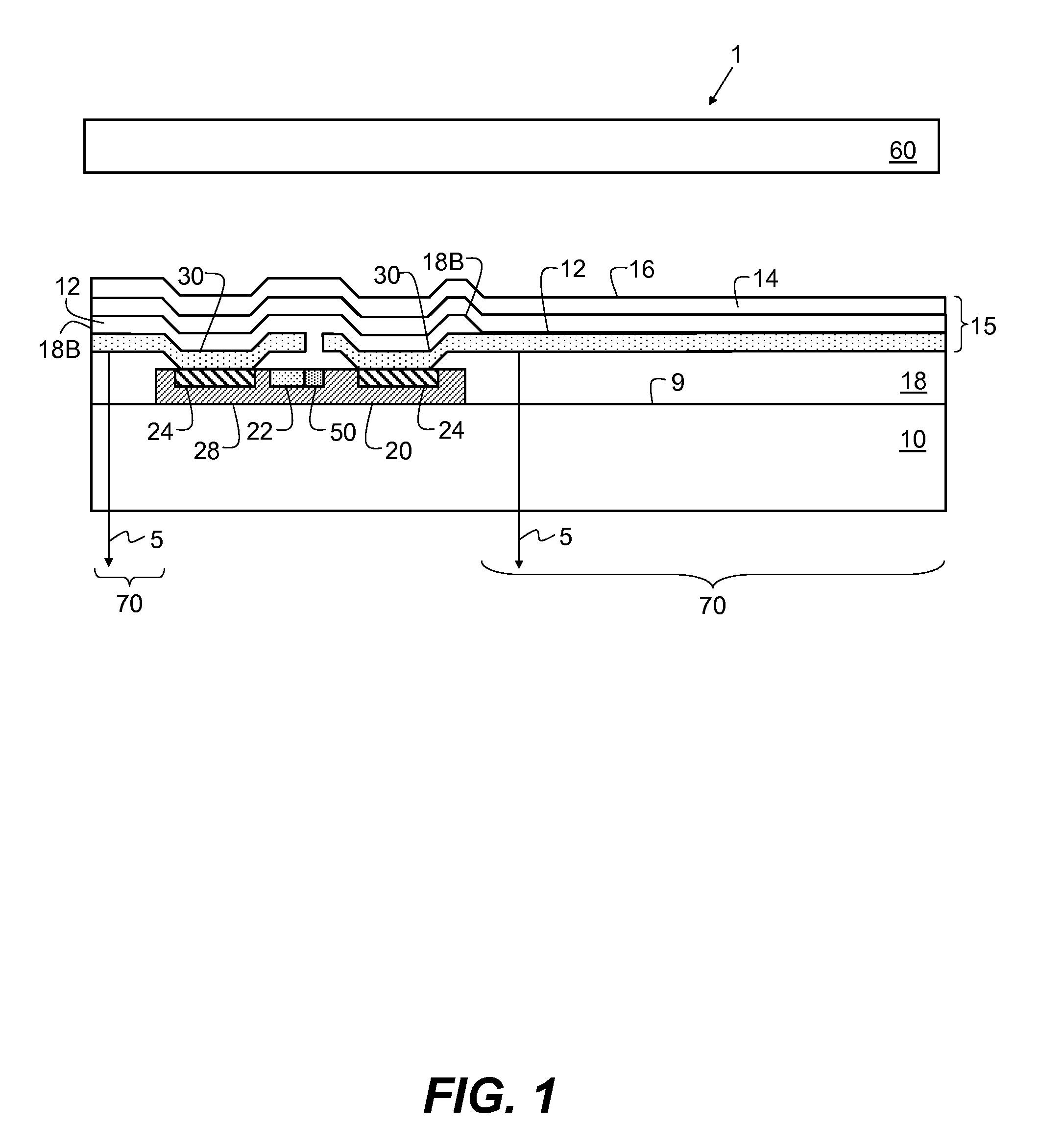
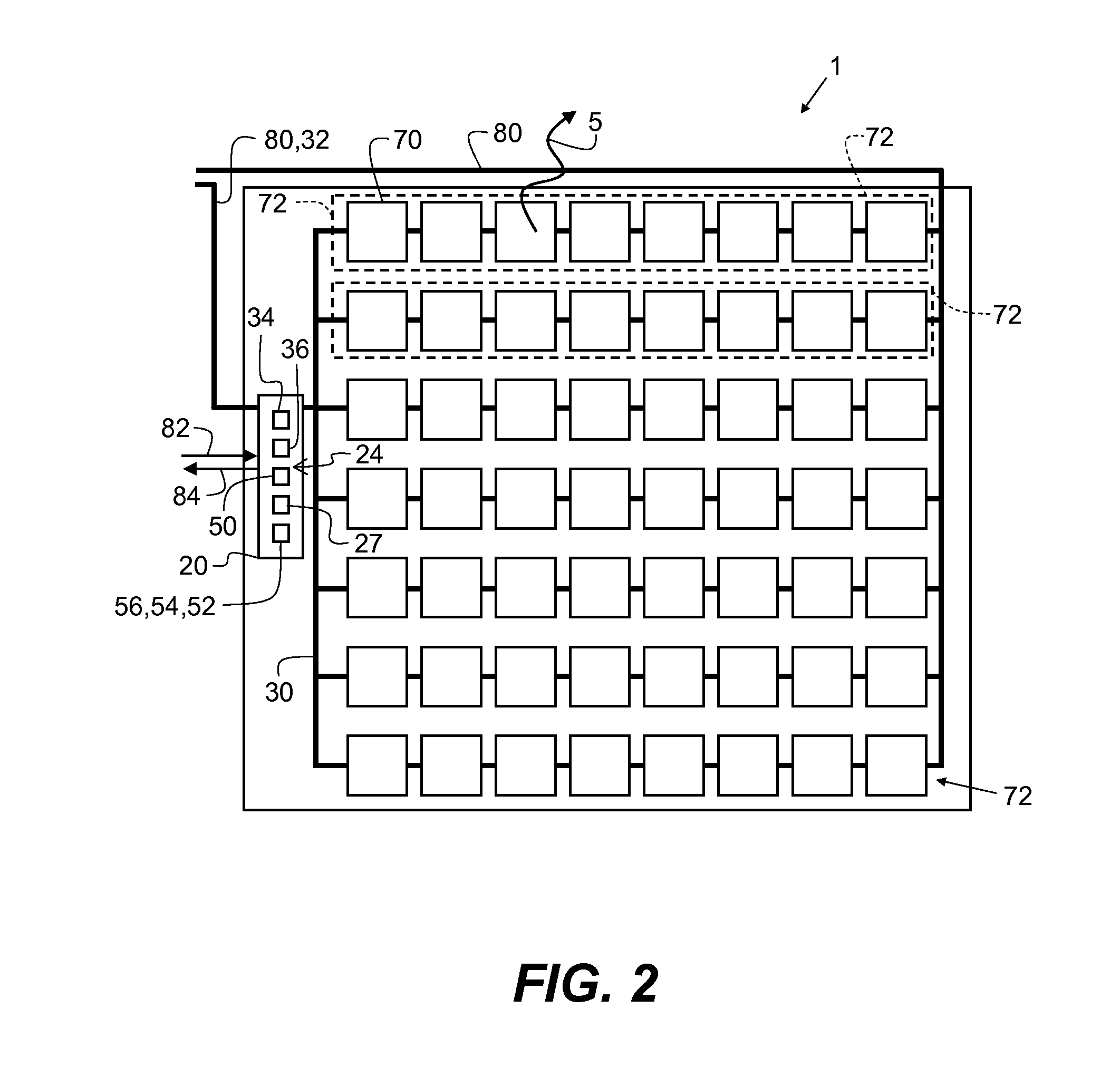
[0029]Referring to FIG. 1, an electroluminescent (EL) lamp 1 includes a lamp substrate 10 having a device side 9. A first electrode 12 is formed over the lamp substrate 10 on device side 9, one or more layers 14 having light-emitting material are formed over the first electrode 12, and a second electrode 16 is formed over the one or more layers 14 of light-emitting material to form a light-emitting diode 15. The first and second electrodes 12, 16 provide current to cause one or more of the layers 14 of light-emitting material to emit light 5 in a light-emitting area 70.

[0030]A chiplet 20 having a chiplet substrate 28 separate and independent from the lamp substrate 10 is located and adhered to the lamp substrate 10 device side 9 with planarization and insulating layers 18 and 18B. The chiplet 20 includes one or more connection pads 24, a mechanical switch 50, and a control circuit 22 formed in the chiplet 20 for controlling the mechanical switch 50. The chiplet 20 is located over, a...


PUM


Abstract

An electroluminescent lam including a lamp substrate; a first electrode formed over the lamp substrate device side, one or more layers having light-emitting material formed over the first electrode, and a second electrode formed over the one or more layers, a chiplet having a chiplet substrate separate and independent from the lamp substrate and adhered to the lamp substrate device side, one or more connection pads, a mechanical switch, and a control circuit for controlling the mechanical switch, the mechanical switch electrically connected to one or more connection pads and at least one connection pad electrically connected to the first or second electrode with one or more electrical connection(s); and an insulating and planarization layer formed over at least a portion of the chiplet and the electrical connections so that the chiplet is an embedded chiplet.

Description

FIELD OF THE INVENTION[0001]The present invention relates to control devices for electroluminescent (EL) lamps.BACKGROUND OF THE INVENTION[0002]Solid-state electroluminescent (EL) lighting devices made of area-emissive light-emitting diodes, both organic and inorganic are increasingly useful for applications requiring robustness and long-life. Such solid-state lighting devices are of great interest because they provide a light-emitting area rather than a point source of light (as is found in inorganic light-emitting diodes formed in crystalline semiconductors). This attribute of EL lighting devices reduces the maximum heat of the device, facilitates efficient extraction of light from the diodes in a lighting fixture or luminaire, and provides large-area diffuse illumination sources, which are preferred in many environments to reduce eye strain and provide a comfortable viewing environment. To obtain these advantages, it is desirable that the luminaire have a large area, typically gr...

Claims


Application Information

Patent Timeline
Patent Type & Authority Applications(United States)
IPC IPC(8): H05B37/02H05B41/36H05B44/00
CPCF21K9/00H01L27/3204H01L27/3255Y02B20/325H01L2251/5361H05B33/08H01L27/3281Y02B20/30H05B45/00H05B44/00H10K59/86H10K59/129H10K59/17H05B33/12
Inventor COK, RONALD S.MILLER, MICHAEL E.
Owner GLOBAL OLED TECH
Why Eureka
Try Eureka