Unlock instant, AI-driven research and patent intelligence for your innovation.

Method for producing reconfigurable microchannels

Inactive Publication Date: 2011-05-05
COMMISSARIAT A LENERGIE ATOMIQUE ET AUX ENERGIES ALTERNATIVES
View PDF45 Cites 6 Cited by
  • Summary
  • Abstract
  • Description
  • Claims
  • Application Information

AI Technical Summary

Benefits of technology

[0010]The invention aims to propose a device which can be produced very easily and which can be rapidly configured as a function of the requirements of a user, without involving cumbersome and laborious manufacturing processes.
[0021]It is then possible to eliminate the first fluid and to replace it with a third fluid, which is for example also liquid and can also be hardened or solidified.
[0024]One and the same component produced according to the invention can therefore be reused a large number of times with a large variety of geometries of microfluidic networks. The formation of each microfluidic network is quick and does not require any micromanufacturing equipment.
[0029]Means may be provided for varying a physical parameter of the material constituting the walls of the channel so as to cause this material to pass at least from the liquid state to the solid state.
[0037]The invention makes it possible to form a microfluidic network of channels in a non-disposable component with the following advantages:
[0041]the material forming the walls can be renewed between each melting, which makes it possible to reuse the component if the microfluidic network has been damaged, contaminated, blocked up, etc.

Problems solved by technology

The manufacture thereof requires equipment of the clean room type, which involves considerable means and long manufacturing times.
This cycle is long (from one week to several months) and expensive, which has a detrimental effect on the progress of a project.
In all the known techniques, the surfaces may be contaminated by chemical or biological reactions and the microfluidic component cannot be reused.
This involves a constraint with regard to a low cost of manufacture, which is unfortunately incompatible with MEMS technologies.

Method used


Image

  • Method for producing reconfigurable microchannels
  • Method for producing reconfigurable microchannels
  • Method for producing reconfigurable microchannels

Examples


Embodiment Construction

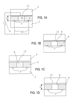
[0056]A first example of embodiment of the invention is shown schematically in FIGS. 1A and 1B.

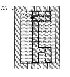
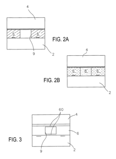
[0057]These figures show, in section, a device comprising two parallel substrates or plates 2, 4, between which a channel 9 is defined. A single channel is shown, but the invention applies to the production of any configuration of channels, for example of the type shown in plan view in any one of FIGS. 12A-12C.

[0058]Two immiscible fluid media 6, 8 are arranged in the space defined between the two parallel plates (or substrates) 2, 4, each of these plates comprising one or more electrodes 3, 13 (FIG. 1A). Hereinbelow, the fluid 6 may be denoted by the expression “first fluid” and the fluid 8 may be denoted by the expression “second fluid”.

[0059]The electrodes may be in direct contact with the medium separating the two plates. This is the case for the electrodes 3, 13 in FIGS. 1A and 1B. The preferred displacement mechanism for the fluids will then be of the DEP (dielectrophoresis) type.

[006...


PUM

PropertyMeasurementUnit
Temperatureaaaaaaaaaa
Dielectric permittivityaaaaaaaaaa

Abstract

A microfluidic device, including a microfluidic network, including: a) two parallel plates each including one or more electrodes, b) at least one channel, arranged between the two plates, made from a material obtained by solidification or hardening of a material of a first fluid, and c) a mechanism varying a physical parameter of the material constituting walls of the channel so as to cause the material to pass at least from the liquid state to the solid state.

Description

TECHNICAL FIELD AND PRIOR ART[0001]The invention relates to the microfluidics field.[0002]In this field, the known devices generally use technologies of the MEMS type. The channels are produced by assembling together two plates, one of the plates having been etched in order to form grooves.[0003]According to another family of devices, a network of microchannels is formed by replication techniques such as the moulding of polymeric materials (for example polycarbonate). Other materials such as PDMS can be cast in micromachined moulds, etc.[0004]In all these known devices, the geometry of the microfluidic network is defined at the time of conception.[0005]The manufacture thereof requires equipment of the clean room type, which involves considerable means and long manufacturing times.[0006]For a new component geometry, it is therefore necessary to carry out a new cycle of conception, production, packaging, etc. This cycle is long (from one week to several months) and expensive, which ha...

Claims


Application Information

Patent Timeline
IPC IPC(8): B01L99/00B81C3/00
CPCB01L3/502707B01L3/50273B01L2200/12B01L2300/0887B82Y30/00B81B2201/051B81C1/00071B81C2201/0149B01L2400/0415
Inventor FOUILLET, YVES
Owner COMMISSARIAT A LENERGIE ATOMIQUE ET AUX ENERGIES ALTERNATIVES