
In-circuit configuration architecture for embedded configurable logic array

Inactive Publication Date: 2005-05-12
MACRONIX INT CO LTD
View PDF47 Cites 31 Cited by
  • Summary
  • Abstract
  • Description
  • Claims
  • Application Information

AI Technical Summary

Benefits of technology

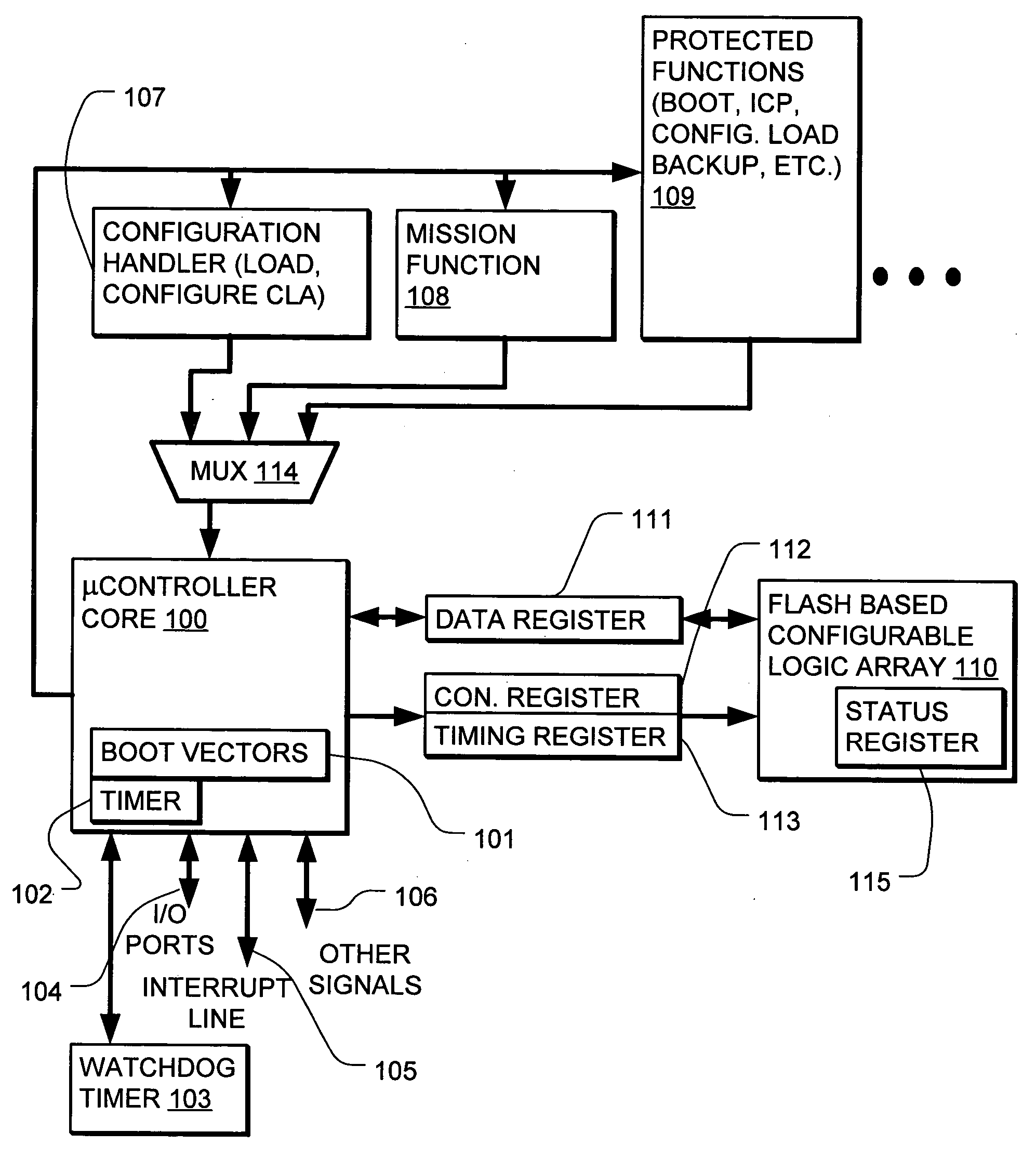
[0015] By providing the instructions for the configuration function and / or the configuration load function on-chip, in a manner configured to be executed by the processor core, the system-on-a-chip integrated circuit of the present invention can be applied easily to a wide variety of environments, in which configuration load of the configurable logic array is desirable.
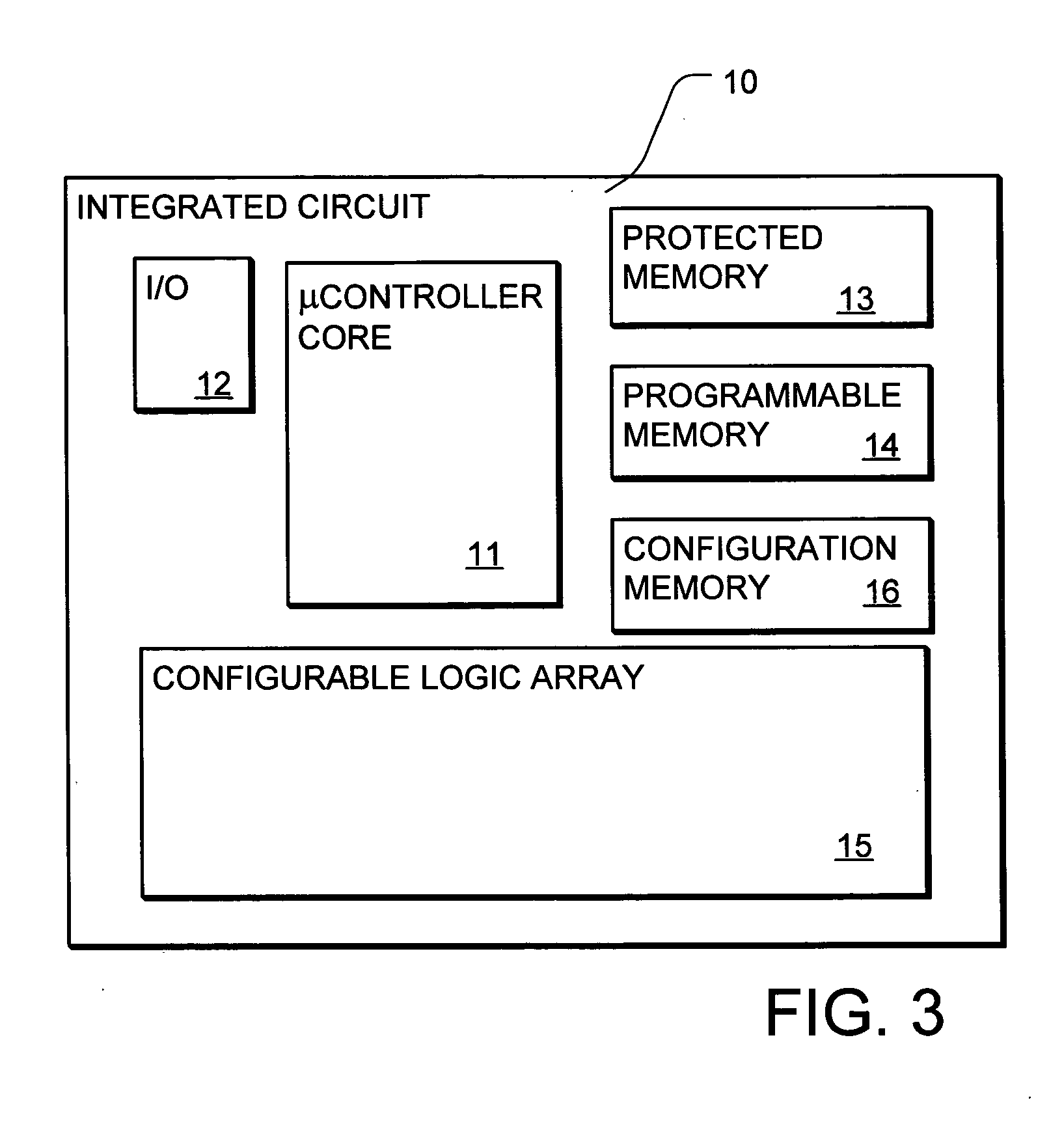
[0020] In some embodiments, a programmable configuration memory is included on the integrated circuit, and adapted to store the configuration data. According to these embodiments, the configuration function includes transferring the configuration data from the configuration memory to the programmable configuration points within the configurable logic array. Also, the configuration load function includes loading the configuration data into the configuration memory from remote sources of data through an input port on the system-on-a-chip integrated circuit. In some embodiments, the programmable configuration memory is implemented using nonvolatile, programmable memory cells, such as floating gate memory, or other charge programmable nonvolatile memory. In some embodiments, the programmable configuration memory is implemented using high-speed SRAM, to support rapid configuration changes of the configurable logic array. Also, some embodiments include both nonvolatile and high-speed volatile memory to support storage and manipulation on-chip of configuration data.

Problems solved by technology

Management of configuration data for the configurable logic array core requires complex logic.
The specialized technology for configuring the devices limits environments in which the technology can be applied.
One problem associated with configurable logic arrays is the loading of configuration data on the chip, while it is mounted on a printed circuit board, or otherwise incorporated into a functioning system.
System-on-a-chip SOC devices increase the complexity of the system even more.
Thus, an SOC system is hard to design and expensive to change.
Nonetheless, the problem of management of configuration data for the configurable logic array modules remains.
SOC technology suffers the classic problem of complex systems, that they are hard to design and expensive to change.

Method used


Image

  • In-circuit configuration architecture for embedded configurable logic array
  • In-circuit configuration architecture for embedded configurable logic array
  • In-circuit configuration architecture for embedded configurable logic array

Examples


Embodiment Construction

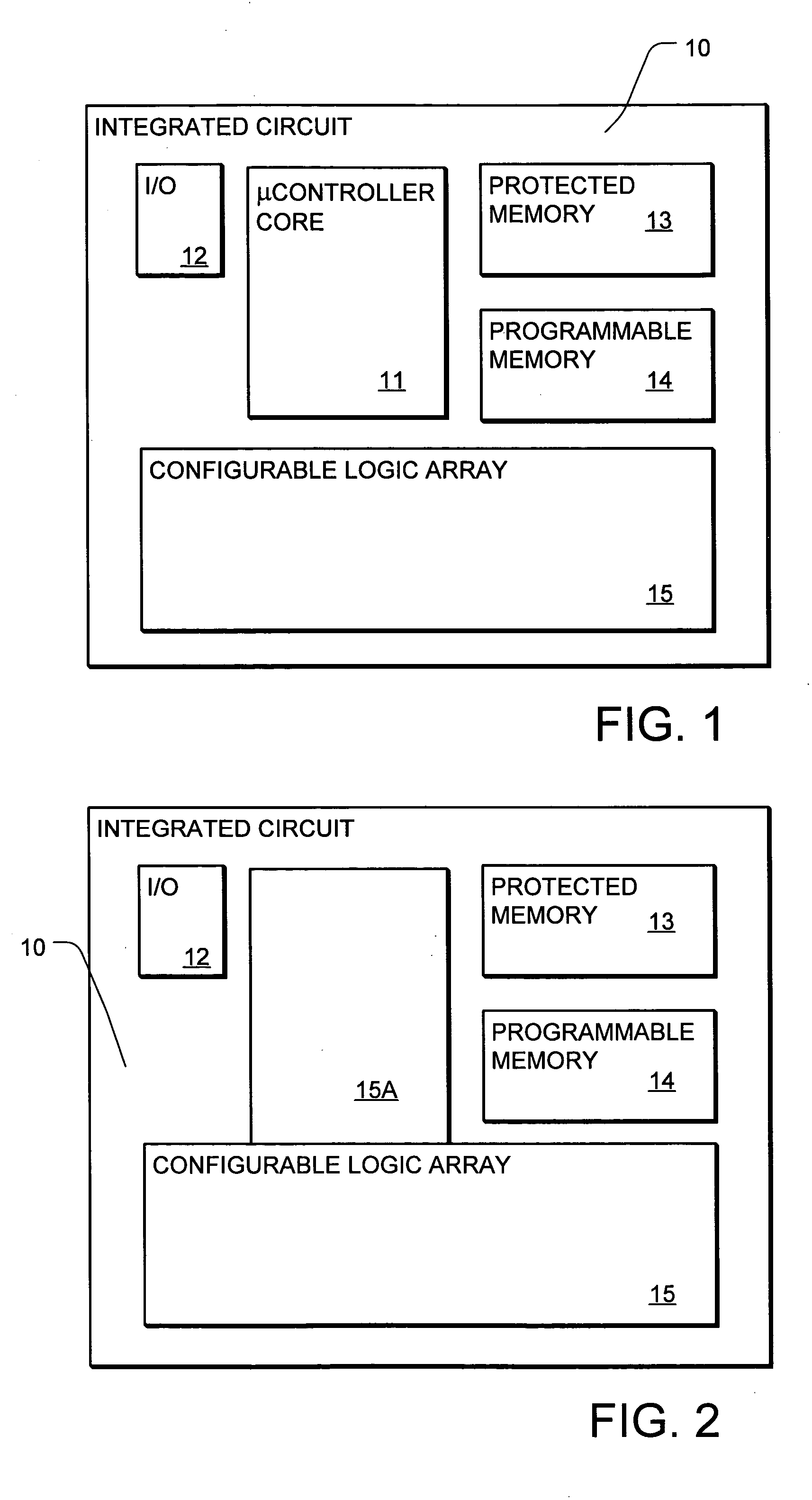
[0032] A detailed description of embodiments of the present invention is provided with reference to FIGS. 1-8. A basic SOC integrated circuit 10 is shown in FIG. 1. The integrated circuit includes a microcontroller core module 11, such as standard 8051 or ARM module as known in the art. In alternatives, the microcontroller core module 11 is replaced or supplemented by other data processor cores, such as digital signal processor cores, high-performance RISC processor cores, or other microprocessor or digital signal processor modules. Protected memory 13 and programmable memory 14 are included on the integrated circuit 10. The protected memory 13 typically stores instructions for boot functions and the like, which are protected from overwriting or modification. The programmable memory 14 typically stores instructions for a mission function for the integrated circuit 10. Input / output structures 12 are included on the integrated circuit 10, supporting one or both of serial and parallel ...


PUM


Abstract

A system-on-a-chip integrated circuit that includes a configurable logic array, a processor core, and a memory adapted to store instructions for a mission function, and instructions for a configuration load function used to load configuration data on to the integrated circuit via an input port on the integrated circuit from an external source. The processor fetches and executes the instructions from the memory. Configuration data received using the configuration load function is used to configure the configurable logic array.

Description

REFERENCE TO RELATED APPLICATION [0001] The present application is related to our co-pending U.S. patent application Ser. No. ______, entitled IN-CIRCUIT CONFIGURATION ARCHITECTURE WITH CONFIGURATION ON INITIALIZATION FUNCTION FOR EMBEDDED CONFIGURABLE LOGIC ARRAY, filed on the same day as the present application; and to our co-pending U.S. patent application Ser. No. ______, entitled IN-CIRCUIT CONFIGURATION ARCHITECTURE WITH NONVOLATILE CONFIGURATION STORE FOR EMBEDDED CONFIGURABLE LOGIC ARRAY, filed on the same day as the present application.BACKGROUND OF THE INVENTION [0002] 1. Field of the Invention [0003] The present invention is related to system-on-a-chip integrated circuits, and other processor devices including embedded configurable logic arrays adapted to be used as application specific or custom on-chip logic. [0004] 2. Description of Related Art [0005] Configurable logic arrays, including for example products known as programmable logic devices PLDs and field programmab...

Claims


Application Information

Patent Timeline
IPC IPC(8): G06F15/78H03K19/173
CPCG06F11/0757G06F15/7867G06F15/7842
Inventor SUN, ALBERTSHEU, ERICCHEN, SHIH-LIANG
Owner MACRONIX INT CO LTD
Learn More