Multilayer ceramic capacitor mounting structure and multilayer ceramic capacitor

a multi-layer ceramic and mounting structure technology, applied in the field of multi-layer ceramic capacitor mounting structure and multi-layer ceramic capacitor, can solve the problems of increasing the height of ripple capacitor and unsuitable for a mounting structure which is limited, and achieve the effect of reducing the frequency of vibration

Active Publication Date: 2011-05-19
TDK CORPARATION
View PDF6 Cites 36 Cited by
  • Summary
  • Abstract
  • Description
  • Claims
  • Application Information

AI Technical Summary

Benefits of technology

[0007]It is an object of the present invention to provide a multilayer ceramic capacitor mounting structure and multilayer ceramic capacitor which can reduce vibration sounds occurring in a substrate without increasing the capacitor mounting area of the substrate and without mounting the capacitor such as to space it from the substrate.
[0008]The inventors conducted diligent studies about vibration sounds occurring when mounting a multilayer ceramic capacitor to a substrate. As a result, the inventors have found a fact that the occurrence of vibration sounds can be reduced by appropriately defining the relationship between the width of a capacitor and the size of a land of the substrate corresponding to the width of the capacitor, the relationship between the height of the capacitor and the outer covering thickness of an element body, the relative permittivity of dielectric layers, and the arranging direction of inner electrodes with respect to a mounting surface of the substrate, thereby completing the present invention.
[0010]In the multilayer ceramic capacitor mounting structure of the present invention, the multilayer ceramic capacitor is mounted such that the inner electrodes are parallel to the mounting surface of the substrate. This seems to make it harder for vibrations generated in the multilayer ceramic capacitor to propagate to the substrate than in the case where the multilayer ceramic capacitor is mounted such that the inner electrodes are perpendicular to the mounting surface of the substrate. Setting the ratio (Tf / T) between the height T of the multilayer ceramic capacitor and the outer covering thickness Tf of the element body to more than 0.1 is also deemed to make it harder for the vibrations generated in the multilayer ceramic capacitor to propagate to the substrate. Setting the relative permittivity ∈r of the dielectric layers to at least 300 but not exceeding 2800 is supposed to make it harder for the vibrations generated in the multilayer ceramic capacitor to propagate to the substrate, while securing the capacity of the multilayer ceramic capacitor. Setting the ratio (Wp / W) between the width W of the multilayer ceramic capacitor and a size Wp of the land in a direction corresponding to the width of the multilayer ceramic capacitor to at least 0.6 but not exceeding 1.0 is speculated to make it harder for the vibrations generated in the multilayer ceramic capacitor to propagate to the substrate, while securing the joint strength between the multilayer ceramic capacitor and the lands. The foregoing can reduce the vibration sounds occurring in the substrate without increasing the capacitor mounting area in order to mount a plurality of multilayer ceramic capacitors to the substrate and without mounting the multilayer ceramic capacitor such as to space it from the substrate.
[0013]When mounting the multilayer ceramic capacitor of the present invention to a substrate, a substrate having a land satisfying 0.6≦Wp / W≦1.0 is used, where W is the width of the multilayer ceramic capacitor, and Wp is the size of the land in a direction corresponding to the width of the multilayer ceramic capacitor. As mentioned above, this can reduce the vibration sounds occurring in the substrate without increasing the capacitor mounting area in order to mount a plurality of multilayer ceramic capacitors to the substrate and without mounting the multilayer ceramic capacitor such as to space it from the substrate.

Problems solved by technology

On the other hand, the structure described in Japanese Patent Application Laid-Open No. 2004-153121 inevitably increases the height of the ripple capacitor, since it is mounted to the substrate so as to space the capacitor body from the substrate surface.
This is unsuitable for a mounting structure which is limited in the height direction.

Method used


Image

  • Multilayer ceramic capacitor mounting structure and multilayer ceramic capacitor
  • Multilayer ceramic capacitor mounting structure and multilayer ceramic capacitor
  • Multilayer ceramic capacitor mounting structure and multilayer ceramic capacitor

Examples


Embodiment Construction

[0023]In the following, preferred embodiments of the multilayer ceramic capacitor mounting structure and multilayer ceramic capacitor in accordance with the present invention will be explained in detail with reference to the drawings.

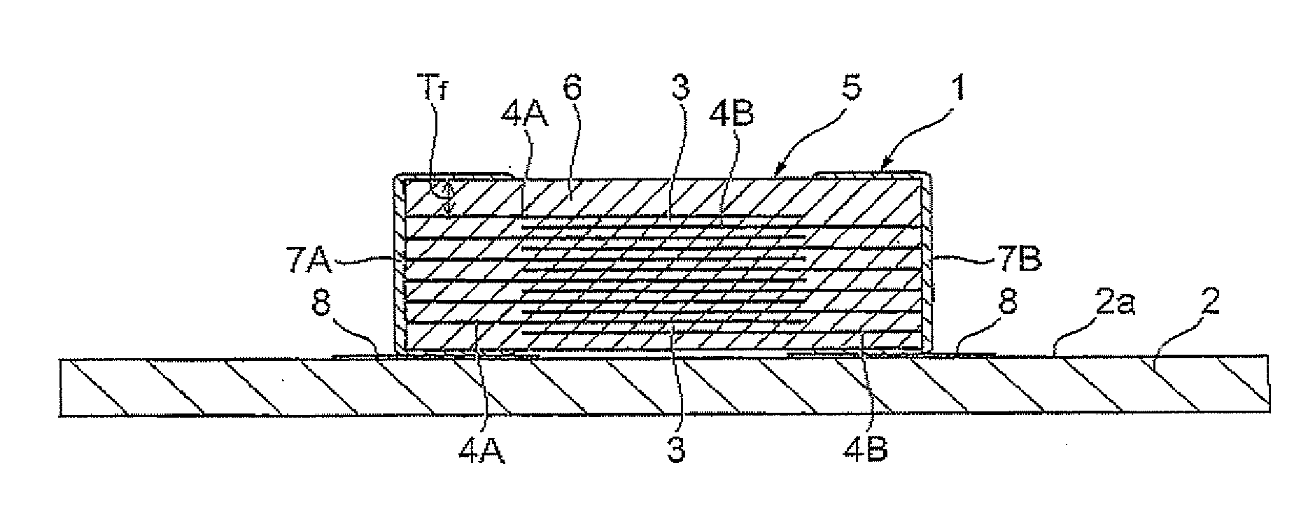
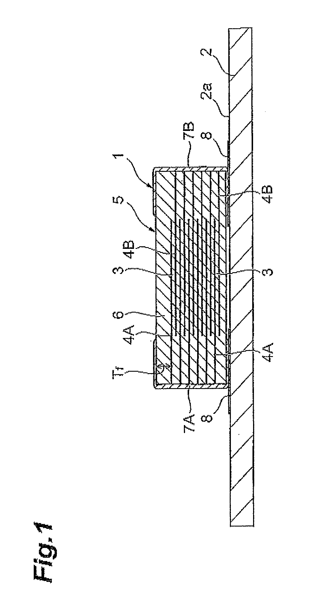
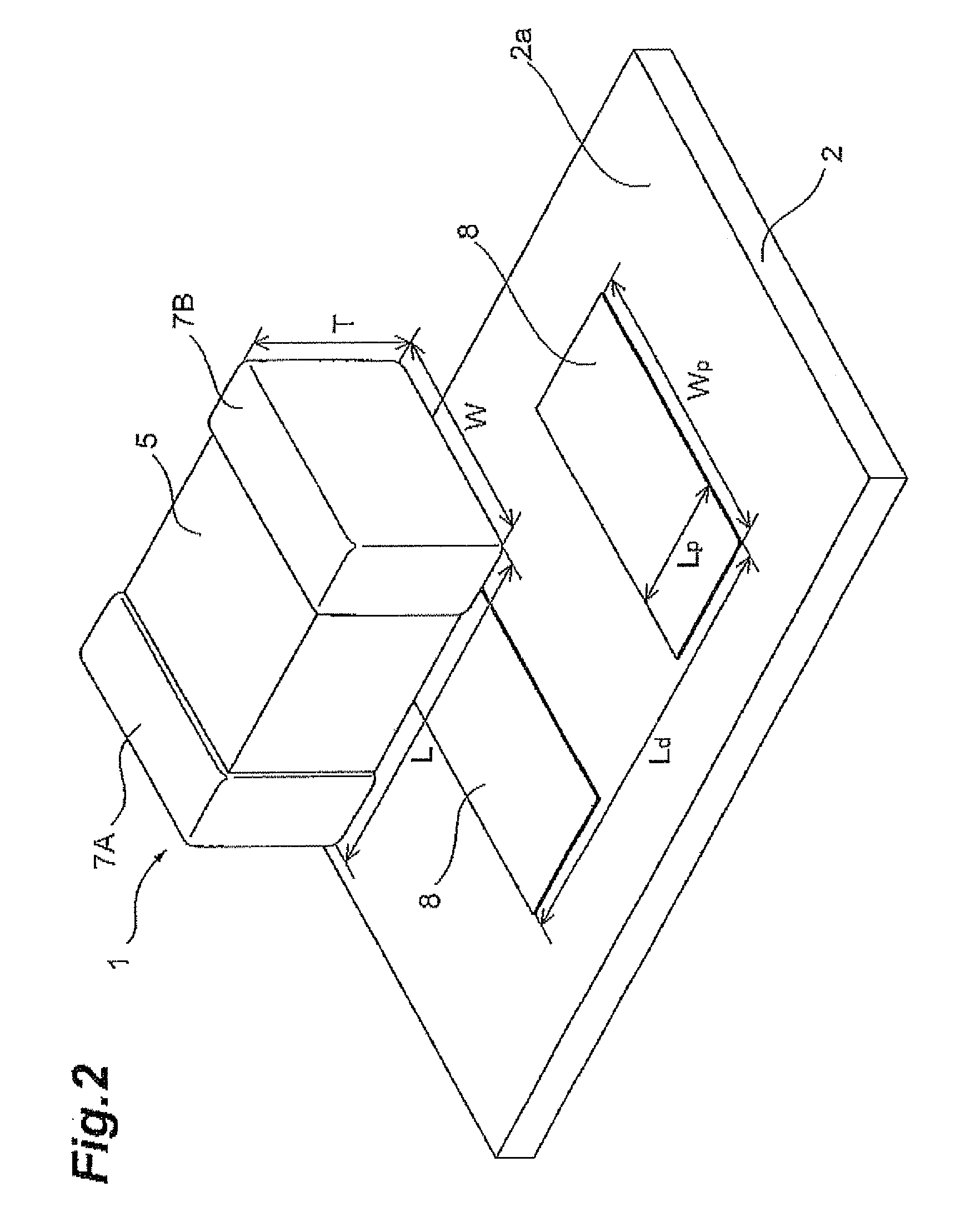
[0024]FIG. 1 is a sectional view showing an embodiment of the multilayer ceramic capacitor mounting structure. FIG. 2 is an exploded perspective view of the multilayer ceramic capacitor mounting structure shown in FIG. 1. In each drawing, the multilayer ceramic capacitor 1 in accordance with this embodiment is mounted to a circuit board 2.

[0025]The multilayer ceramic capacitor 1 has a rectangular parallelepiped capacitor element body 5 constituted by a plurality of dielectric layers 3 and a plurality of inner electrodes 4A, 4B. The capacitor element body 5 has a structure in which the inner electrodes 4A, 413 are laminated alternately with the dielectric layers 3. The inner electrodes 4A are drawn to one end face of the capacitor element body 5, while t...


PUM

PropertyMeasurementUnit
relative permittivity ∈raaaaaaaaaa
relative permittivityaaaaaaaaaa

Abstract

A multilayer ceramic capacitor has an element body formed by alternately laminating a plurality of dielectric layers and a plurality of inner electrodes. On a substrate having a mounting surface provided with at least two lands, the multilayer ceramic capacitor is mounted such that the inner electrodes are parallel to the mounting surface. A multilayer ceramic capacitor mounting structure satisfies Tf / T>0.1 and 300≦∈r≦2800, where T is the height of the multilayer ceramic capacitor, Tf is the outer covering thickness of the element body, and ∈r is the relative permittivity of the dielectric layers, and 0.6≦Wp / W≦1.0, where W is the width of the multilayer ceramic capacitor, and Wp is the size of the land in a direction corresponding to the width of the multilayer ceramic capacitor.

Description

BACKGROUND OF THE INVENTION[0001]1. Field of the Invention[0002]The present invention relates to a multilayer ceramic capacitor mounting structure for mounting a multilayer ceramic capacitor to a substrate and a multilayer ceramic capacitor.[0003]2. Related Background Art[0004]Known as examples of conventional multilayer ceramic capacitor mounting structures are those disclosed in Japanese Patent Application Laid-Open Nos. 2002-232110 and 2004-153121. The mounting structure described in Japanese Patent Application Laid-Open No. 2002-232110 is constructed such that a plurality of ceramic capacitors are arranged in a row on a circuit board, while respective vibrations generated in dielectric layers of the ceramic capacitors and then transmitted to the circuit board have substantially opposite phases. This inhibits the circuit board from generating vibration sounds.[0005]The mounting structure described in Japanese Patent Application Laid-Open No. 2004-153121 constructs a ripple capaci...

Claims


Application Information

Patent Timeline
Patent Type & Authority Applications(United States)
IPC IPC(8): H05K1/16H01G4/06
CPCH01G2/065H01G4/232H01G4/30H05K1/0271H05K2201/2045H05K3/3442H05K2201/10015H05K2201/10636H05K1/181Y02P70/50
Inventor YOSHII, AKITOSHIHASEBE, KAZUYUKIKUBO, KEIKOKATAOKA, NARUKI
Owner TDK CORPARATION
Why Eureka
Try Eureka