Delay compensation for a dc-dc converter
- Summary
- Abstract
- Description
- Claims
- Application Information
AI Technical Summary
Benefits of technology
Problems solved by technology
Method used
Image

Examples
Embodiment Construction
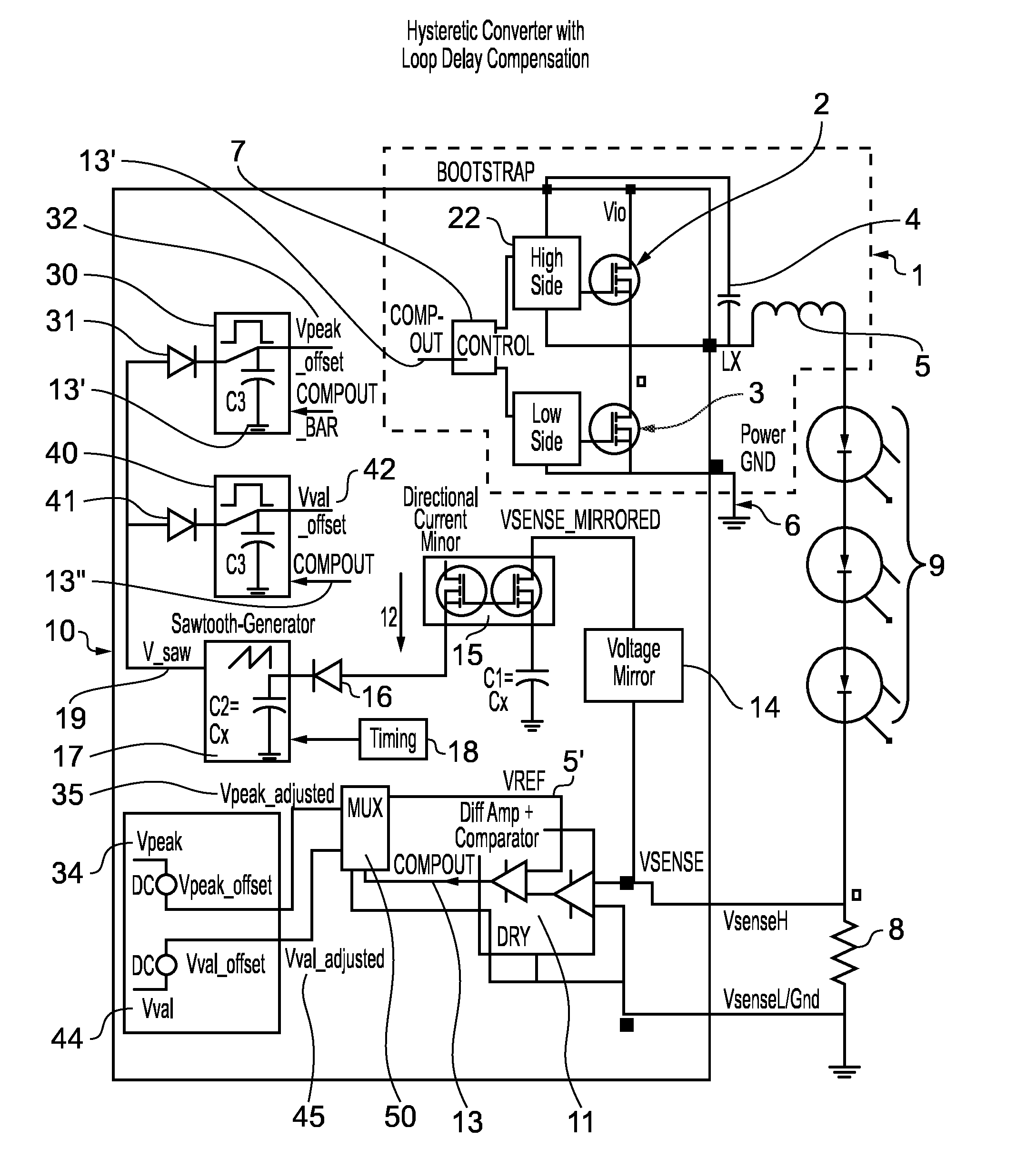
[0035]FIG. 1 shows a hysteretic converter with loop delay compensation. The basic converter shown in region 1 comprises high side switch 2 and low side switch 3 connected in series between supply voltage Vin and ground level 4. The midpoint node LX between high side switch 2 and low side switch 3 is connected to capacitor 4 and to one terminal of an inductor 5. High side switch 2 and low side switch 3 are driven by respective drivers 22 and 32; these are both controlled by controller 7.
[0036]The output current from the inductor 5 is sensed by means of senses resistor 8, which is connected between load 9 and ground.
[0037]In this particular example the load 9 is shown as a string of lights emitting diodes (LEDs); however, the load is not limited to LEDs, and could be, for example, fluorescent lamps, battery which is being charged, PC circuitry, mobile device electronics and the like. In each case, the current sensing resistor has to be placed at the appropriate location to get the act...
PUM
 Abstract
Description
Claims
Application Information
 - R&D Engineer
- R&D Manager
- IP Professional
- Industry Leading Data Capabilities
- Powerful AI technology
- Patent DNA Extraction
Browse by: Latest US Patents, China's latest patents, Technical Efficacy Thesaurus, Application Domain, Technology Topic.
© 2024 PatSnap. All rights reserved.Legal|Privacy policy|Modern Slavery Act Transparency Statement|Sitemap