Semiconductor Package and Manufacturing Methods Thereof

a technology of semiconductor devices and manufacturing methods, applied in the direction of semiconductor devices, semiconductor/solid-state device details, electrical apparatus, etc., can solve the problems of reducing the size of the device, and reducing the complexity of the semiconductor devi

Inactive Publication Date: 2011-06-02
ADVANCED SEMICON ENG INC
View PDF158 Cites 81 Cited by
  • Summary
  • Abstract
  • Description
  • Claims
  • Application Information

AI Technical Summary

Problems solved by technology

Semiconductor devices have become progressively more complex, driven at least in part by the demand for smaller sizes and enhanced processing speeds.
While the benefits of smaller sizes and enhanced processing speeds are apparent, these characteristics of semiconductor devices also can crea

Method used


Image

  • Semiconductor Package and Manufacturing Methods Thereof
  • Semiconductor Package and Manufacturing Methods Thereof
  • Semiconductor Package and Manufacturing Methods Thereof

Examples


Embodiment Construction

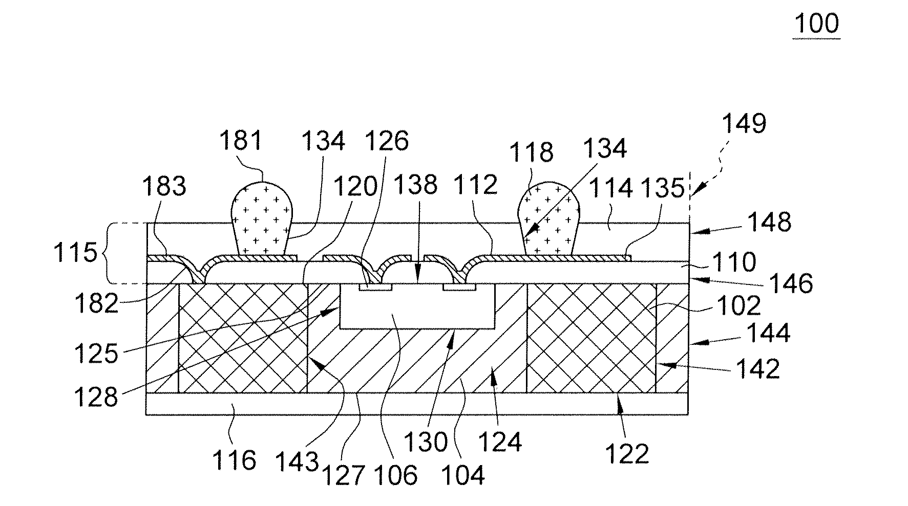
[0026]Referring to FIG. 1, a cross-sectional view of a semiconductor package 100 according to an embodiment of the invention is shown. The semiconductor package 100 may be a communication semiconductor package or another type of semiconductor package. The semiconductor package 100 includes an electromagnetic interference shield including a lateral section 102 and a central section 116, a package body 104, a die 106, a redistribution layer 115, an electrical contact 118, and an electrical contact 181. The redistribution layer 115 includes a first dielectric layer 110, a conductive layer 112, and a second dielectric layer 114. The thickness of the lateral section 102 may be substantially equal to the thickness of the package body 104.

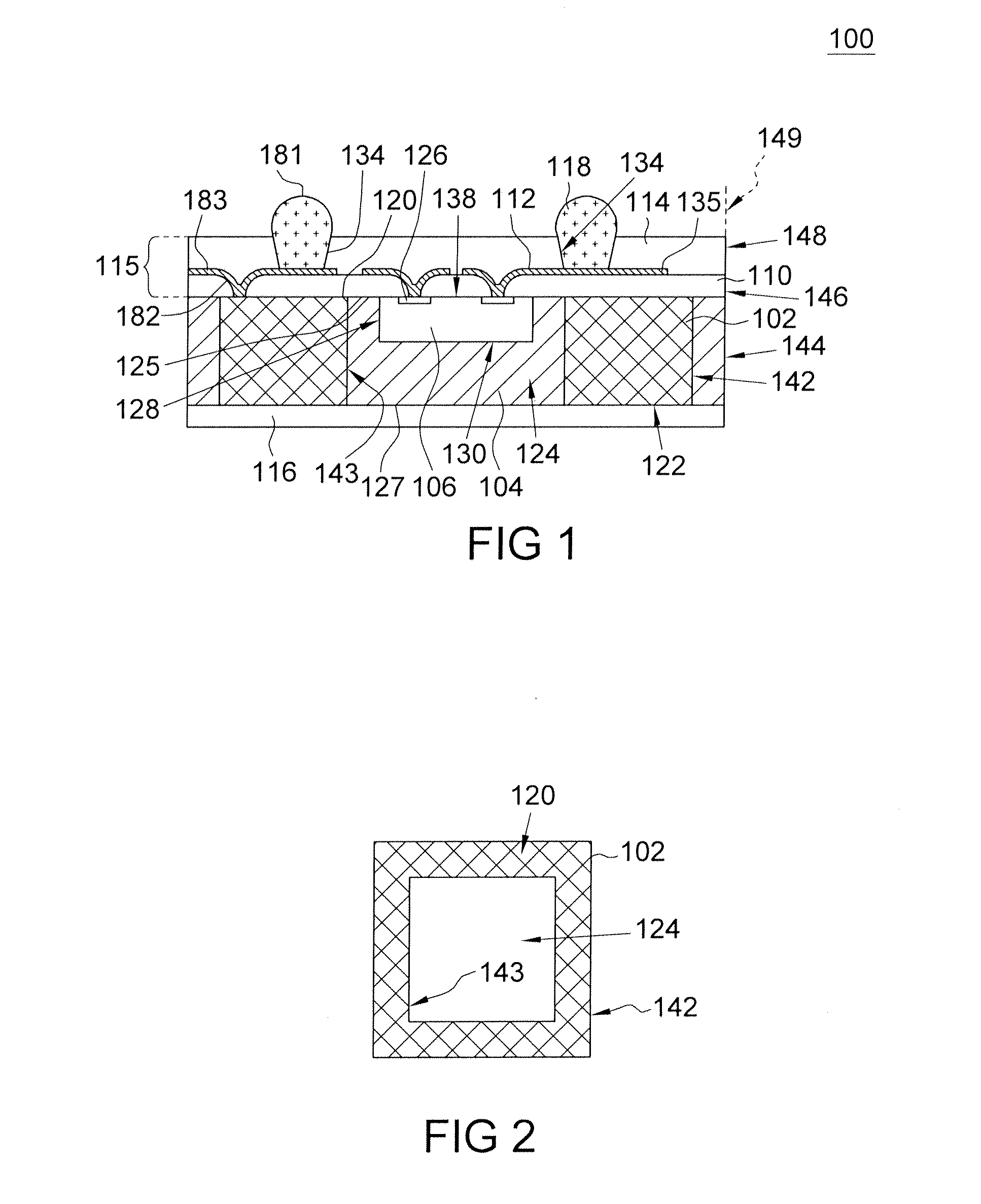
[0027]FIG. 2 is a top view of the lateral section 102 of the electromagnetic interference shield of FIG. 1, according to an embodiment of the invention. Referring to both FIG. 1 and FIG. 2, the lateral section 102 includes a first surface 120, a second su...


PUM


Abstract

A semiconductor package and manufacturing methods thereof are provided. In one embodiment, the semiconductor package includes a die, a shield, a package body, and a redistribution layer. The die has an active surface and an inactive surface. The shield is disposed over the inactive surface of the die. The package body encapsulates the die and a first portion of the shield, where a first surface of the package body is substantially coplanar with the active surface of the die. The redistribution layer is disposed on the active surface of the die and on portions of the first surface of the package body.

Description

CROSS-REFERENCE TO RELATED APPLICATION[0001]The present application claims the benefit of Taiwan Application No. 98140649, filed on Nov. 27, 2009, the subject matter of which is incorporated herein by reference.BACKGROUND OF THE INVENTION[0002]1. Field of the Invention[0003]The present invention generally relates to electronic device packaging. More particularly, the present invention relates to a semiconductor package and manufacturing methods thereof.[0004]2. Description of Related Art[0005]Semiconductor devices have become progressively more complex, driven at least in part by the demand for smaller sizes and enhanced processing speeds. While the benefits of smaller sizes and enhanced processing speeds are apparent, these characteristics of semiconductor devices also can create problems.[0006]In conventional wafer-level packaging, semiconductor devices within a wafer are packaged prior to singulation of the wafer. As such, conventional wafer-level packaging can be restricted to a...

Claims


Application Information

Patent Timeline
IPC IPC(8): H01L23/552H01L21/56
CPCH01L21/568H01L21/6835H01L2924/1461H01L2224/92244H01L2224/32245H01L2224/73267H01L2924/014H01L23/3128H01L23/49816H01L23/5389H01L23/552H01L24/19H01L24/20H01L24/29H01L24/96H01L24/97H01L2221/68359H01L2224/04105H01L2224/20H01L2224/97H01L2924/01013H01L2924/01029H01L2924/01079H01L2924/01082H01L2924/078H01L2924/14H01L2924/15153H01L2924/15165H01L2924/15173H01L2924/15311H01L2924/16152H01L2924/167H01L2924/3025H01L2924/01005H01L2924/01006H01L2924/01033H01L2924/01075H01L2224/82H01L2924/00H01L2224/12105H01L2224/18H01L2924/181
Inventor WENG, CHAOFUHUNT, JOHN RICHARDTSAI, LI CHUANWU, YI TINGFU, CHIEH-CHENOU, YING-TE
Owner ADVANCED SEMICON ENG INC
Why Eureka
Try Eureka