Stackable semiconductor device and fabrication method thereof

a technology of semiconductor devices and stacking dies, applied in semiconductor devices, semiconductor/solid-state device details, electrical apparatus, etc., can solve the problems of reducing size, increasing cost, and reducing method size, so as to avoid poor electrical quality, increase electrical functionalities, and not increase the area of stacked dies

Inactive Publication Date: 2008-09-25
SILICONWARE PRECISION IND CO LTD
View PDF4 Cites 32 Cited by
  • Summary
  • Abstract
  • Description
  • Claims
  • Application Information

AI Technical Summary

Benefits of technology

[0009]In the light of forgoing drawbacks, an objective of the present invention is to provide a stackable semiconductor device and a fabrication method thereof that enables integration of multiple dies in a single semiconductor package without increasing the area of the stacked dies.
[0010]Another objective of the present invention is to provide a stackable semiconductor device and a fabrication method thereof that is simpler and cheaper to implement than the conventional TSV technique.
[0011]Still another objective of the present invention is to provide a stackable semiconductor device and a fabrication method thereof that allows a plurality of semiconductor dies to directly electrically connect each other, avoiding poor electrical quality associated with the conventional wire bonding technique.
[0017]Subsequently, the second metal layer on the non-active face of a first semiconductor device can be attached and electrically connected to a die carrier, while the second metal layer on the non-active face of a second semiconductor device can be attached and electrically connected to the first metal layer on the active face of the first semiconductor device, thereby obtaining a stackable multi-die structure. In this way, a plurality of dies can be vertically stacked on one another to increase electrical functionalities while not increasing the area of the stacked dies, at the same time avoiding poor electrical quality associated with the conventional wire bonding technique and complexity and high cost involved with TSV technique.

Problems solved by technology

As such, a considerable large die attachment area has to be provided for multi-die designs; this will result in cost increase and limitation in size reduction.
This method saves more space than the conventional semiconductor package with horizontally arranged dies.
However, it still requires the use of bonding wires to electrically connect the dies and the substrate.
As a result, the quality of electrical connection may be adversely affected by the length of the wires.
Moreover, since the dies still have to be offset to some extent to allow wire bonding, the die attachment area cannot be minimized.
However, these techniques require complicated and expansive manufacturing processes.

Method used


Image

  • Stackable semiconductor device and fabrication method thereof
  • Stackable semiconductor device and fabrication method thereof
  • Stackable semiconductor device and fabrication method thereof

Examples


first embodiment

[0026]Referring to FIGS. 3A to 3I, a stackable semiconductor device and a fabrication method thereof according to a first embodiment of the present invention is depicted.

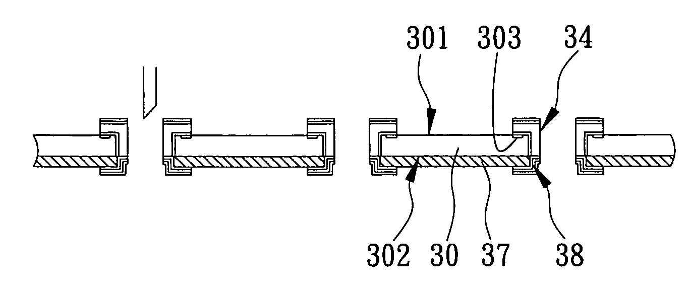
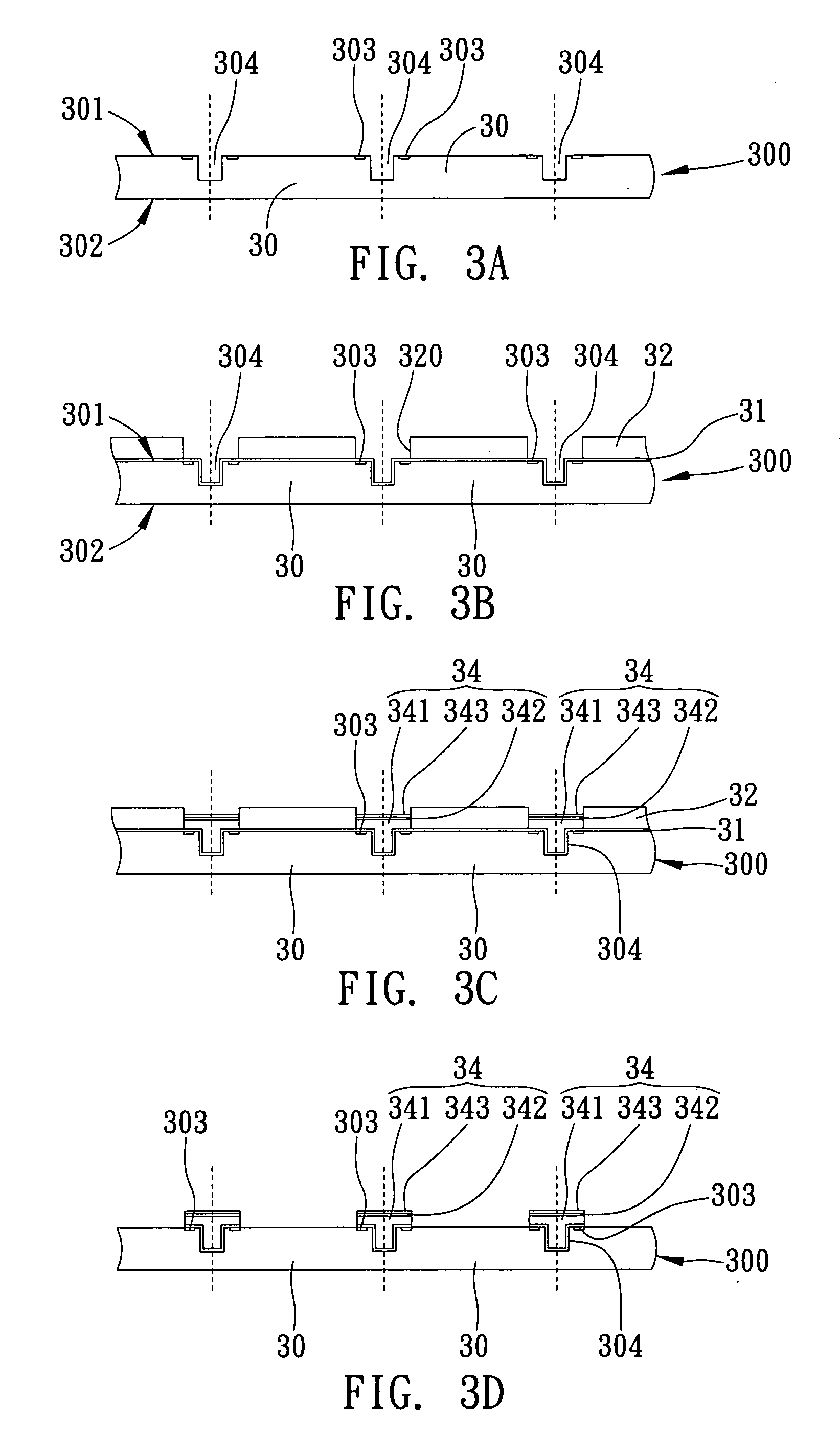
[0027]As shown in FIG. 3A, a wafer 300 with a plurality of dies 30 is provided. The dies 30 and the wafer 300 have an active face 301 and a non-active face 302. A plurality of solder pads 303 is disposed on the active face 301 of the dies 30. Grooves 304 are formed between two neighboring solder pads 303.

[0028]As shown in FIGS. 3B to 3D, a conductive layer 31 is formed on the active face 301 using methods such as sputtering. The conductive layer 31 can be made of materials such as Ti / Cu, TiW / Cu, TiW / Au, Al / NiV / Cu, NiV / Cu, Ti / NiV / Cu or TiW / NiV / Cu. Then, a resist layer 32 is further formed on the conductive layer 31 with a plurality of openings 320 that correspondingly expose the grooves 304.

[0029]Then, electroplating is performed to form a first metal layer 34 in the grooves 34 inside the resist openings 320. The fir...

second embodiment

[0038]Referring to FIG. 5, a cross-section view of a stackable semiconductor device according to a second embodiment of the present invention is depicted. The semiconductor device of this embodiment is similar to that of the previous embodiment, the main difference being that the first metal layer 44 electroplated on the active face 401 of the die 40 is made of gold (Au), facilitated by pre-sputtering the conductive layer 41 (e.g. TiW / Au) on the active face 401. It has a thickness of about 15˜30 m. Additionally, the second metal layer 48 electroplated on the non-active face 402 is made of tin (Sn) or gold (Au), facilitated by pre-sputtering the conductive layer 41′ (e.g. Ti / Cu, TiW / Cu or TiW / Au) on the non-active face 402. It has a thickness of about 20˜40 m.

[0039]As a result, during stacking, the second metal layer (e.g. tin) of one semiconductor device can be directly thermally compressed onto the first metal layer (e.g. gold) of another semiconductor device, thus forming a eutect...

third embodiment

[0041]Referring to FIGS. 6A to 6D, a cross-section view of a stackable semiconductor device according to a third embodiment of the present invention is depicted. For simplicity, elements in this embodiment that are the same or similar to those in the first embodiment are designated by the same reference number.

[0042]The semiconductor device of this embodiment is similar to that of the first embodiment, the main difference being that, after forming grooves 304 between the adjacent solder pads 303, an insulating layer of polymer gel 310 is further formed in the grooves 304. The polymer gel 310 forms dents 304′. Then, a conductive layer 31 is formed on the active face 301 of the wafer 300, the dents 304′ and in the grooves 304, thus forming the polymer gel 310 between the die 30 and the conductive layer 31. The polymer gel 310 can be made of materials such as polyimide (PI) or benzocyclobutene (BCB). The polymer gel 310 increases insulation and adhesion between the die 30 and the condu...


PUM


Abstract

The invention provides a stackable semiconductor device and a fabrication method thereof, including providing a wafer having a plurality of dies mounted thereon, both the die and the wafer having an active surface and a non-active surface opposing one another respectively, wherein each die has a plurality of solder pads formed on the active surface thereof and a groove formed between adjacent solder pads to form a first metal layer therein that is electrically connected to the solder pads; subsequently thinning the non-active surface of the wafer to where the grooves are located to expose the first metal layer therefrom, and forming a second metal layer on the non-active surface of the wafer for electrically connecting with the first metal layer; and separating the dies to form a plurality of stackable semiconductor devices. Thereby, the first and second metal layers formed on the active surface and the non-active surface of the semiconductor device can be stacked and connected to constitute a multi-die stack structure, thereby increasing integration without increasing the area of the stacked dies. Further, the problems known in the prior art of poor electrical connection, complicated manufacturing process and increased cost as a result of using wire bonding and TSV can be avoided.

Description

FIELD OF THE INVENTION[0001]The present invention relates to a semiconductor device and a fabrication method thereof, and more particularly, to a vertically stackable semiconductor device and a fabrication method thereof.BACKGROUND OF THE INVENTION[0002]As the need for portable electronic products and associated products (e.g. in communication, network and computer applications) to become more compact and lighter increases, accompanied by the trend for multi-functional and high-performance electronic devices, conventional semiconductor packages are manufactured in Multichip Module (MCM) to achieve high integration and miniaturization, wherein at least two dies are attached to a substrate (or lead frame) of a single package.[0003]Referring to FIG. 1, a conventional semiconductor package having a plurality of horizontally spaced dies is depicted. This semiconductor package includes a substrate 100, a first die 110 having an active face 110a electrically connected to the substrate 100 ...

Claims


Application Information

Patent Timeline
Patent Type & Authority Applications(United States)
IPC IPC(8): H01L23/488H01L21/304
CPCH01L21/6835H01L21/76898H01L2924/014H01L2924/01033H01L2924/01023H01L2924/00013H01L24/48H01L2924/01322H01L2924/01082H01L2924/01079H01L2924/01074H01L2924/01029H01L2924/01022H01L2924/01013H01L2225/06562H01L21/78H01L23/481H01L24/11H01L24/12H01L24/81H01L25/0657H01L25/50H01L2221/68372H01L2224/1147H01L2224/1184H01L2224/1308H01L2224/13083H01L2224/13111H01L2224/13144H01L2224/13147H01L2224/13155H01L2224/2518H01L2224/48091H01L2224/48227H01L2224/81203H01L2224/81801H01L2225/06513H01L2225/06551H01L2924/00014H01L2224/13099H01L2224/05001H01L2224/05147H01L2224/05155H01L2224/05611H01L24/13H01L2224/0231H01L24/05H01L24/03H01L2224/02371H01L2224/05548H01L2224/45099H01L2224/45015H01L2924/207
Inventor HUANG, CHIEN-PINGCHANG, CHIN-HUANGHUANG, CHIH-MINGKE, CHUN-CHI
Owner SILICONWARE PRECISION IND CO LTD
Why Eureka
Try Eureka