Chip and manufacturing method thereof

Active Publication Date: 2008-04-17
ADVANPAK SOLUTIONS PTE
View PDF16 Cites 30 Cited by
  • Summary
  • Abstract
  • Description
  • Claims
  • Application Information

AI Technical Summary

Benefits of technology

[0011]According to an aspect of an embodiment of the invention, a semiconductor device and a manufacturing method thereof are provided. The first dimension of the bump is longer than 1.2 times the second dimension, or the width of the extension of the bump is longer than 1.2 times the width of the bonding pad, such that the semiconductor device an

Problems solved by technology

Consequently, the semiconductor device can not be firmly assembled on the flip-chip carrier.
To the worse, shortcircuit may occur, severely affecting the electrical functions of the packing structure.
The above defected semiconductor device 900 is hard to be re-worked, and is thus wasted.
In case the defected semiconductor device 900 can be re-worked, the cost involved is expensive

Method used


Image

  • Chip and manufacturing method thereof
  • Chip and manufacturing method thereof
  • Chip and manufacturing method thereof

Examples


first embodiment

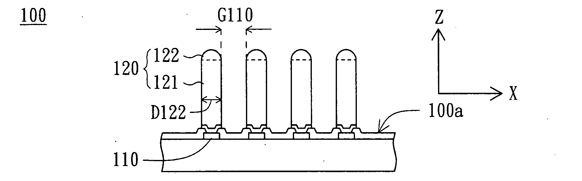
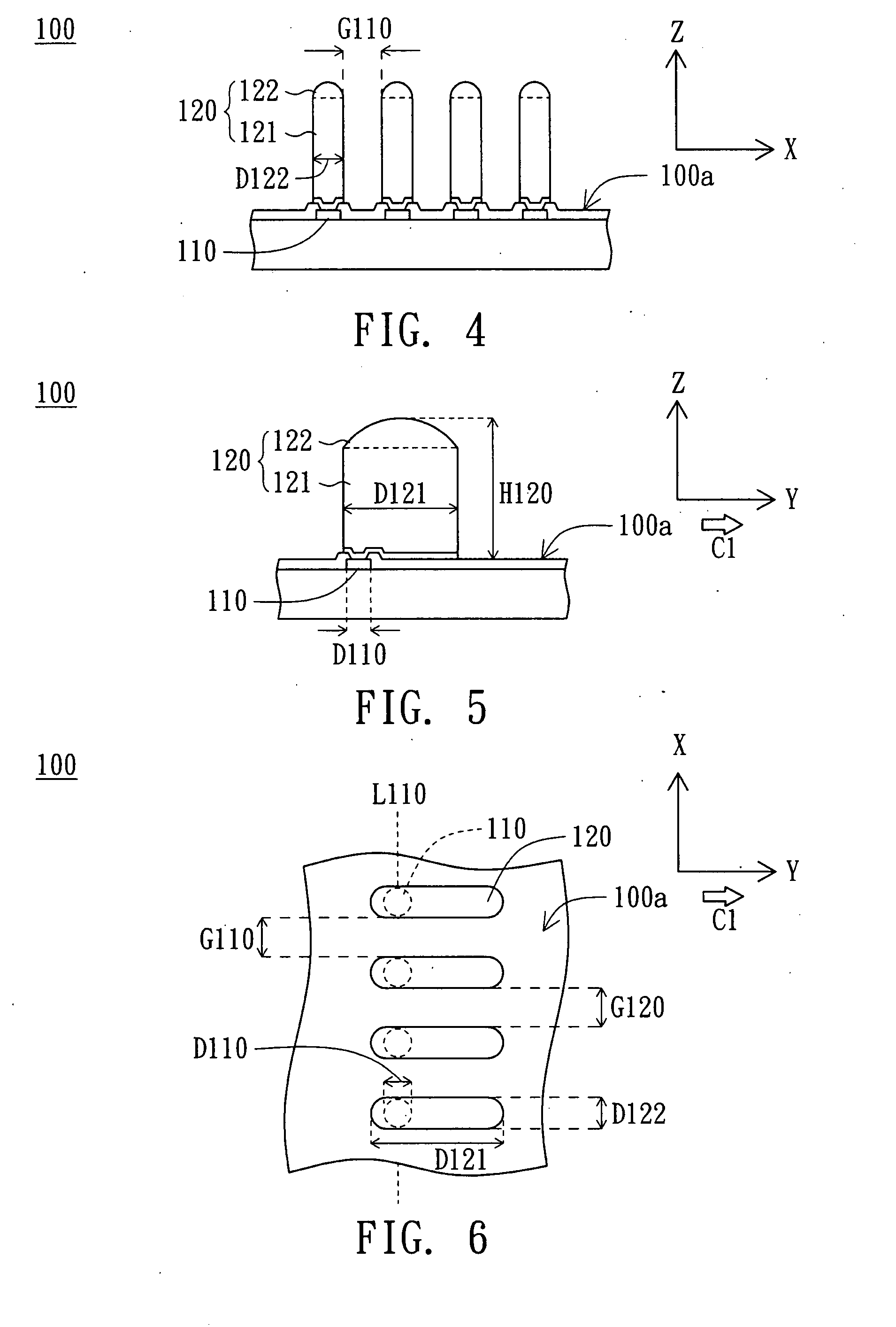
[0030]Referring to both FIG. 4˜6. FIGS. 4˜5 are side views of a semiconductor device 100 according to a first embodiment of the invention. FIG. 6 is a top view of a semiconductor device of FIGS. 4˜5. As indicated in FIG. 4, the semiconductor device 100 has an active surface 100a and includes at least a bonding pad 110 and at least a bump 120. The bonding pad 110 disposed on the active surface 100a is a connecting element for electrically connecting the active surface 100a to the bump 120. The bump 120 is vertically disposed on the bonding pad 110. As indicated in FIG. 6, the bump has a first dimension D121 and a second dimension D122 both parallel to the active surface 100a, wherein the first dimension D121 is illustrated in FIG. 5 and FIG. 6, and the second dimension D122 is illustrated in FIG. 4 and FIG. 6. The first dimension D121 is longer than 1.2 times the second dimension D122. As the structural strength of miniaturized elements is emphasized in the present embodiment of the ...

second embodiment

[0054]The semiconductor device 200 and manufacturing method thereof of the present embodiment of the invention differs with the semiconductor device 100 and manufacturing method thereof of the first embodiment in the disposition of the bump 220, and other similarities are not repeated here. Referring to FIG. 11, the disposition of a bump 220 of a semiconductor device 200 according to a second embodiment of the invention is shown. In the present embodiment of the invention, the semiconductor device 200 includes a plurality of bonding pads 110 and bumps 220. Each of the bumps 220 corresponds to each of the bonding pads 110, and the directions C1 and C2 in which the bumps 220 extend from the bonding pads 110 are substantially parallel to each other. The bonding pads 110 are arranged along a line L110, and the bumps 220 alternately extend in opposite directions C1 and C2 from the bonding pads 110 to form a fan-out arrangement.

[0055]There is a larger pitch G220 between the bumps 220 exte...

third embodiment

[0058]The semiconductor device 300 and manufacturing method thereof of the present embodiment of the invention differs with the semiconductor device 200 and manufacturing method thereof of the second embodiment in the structural design of the bump 320, and other similarities are not repeated here. Referring to FIG. 12, the disposition of a bump 320 of a semiconductor device 300 according to a third embodiment of the invention is shown. In the present embodiment of the invention, the bump 320 of the semiconductor device 300 has a substantially T-shaped cross-section parallel to the active surface 300a.

[0059]As indicated in FIG. 12, after the T-shaped bump 320 substantially extends a first distance D31 in a first direction C31 from the bonding pad 110, the bump 320 extends a second distance D32 in a second direction C32 and a third direction C33 respectively. The first distance D31 is longer than 1.2 times the width D110 of the bonding pad 110.

[0060]The cross-section of the bump is e...


PUM


Abstract

A semiconductor device and a manufacturing method thereof are provided. The semiconductor device has an active surface. The semiconductor device includes at least a connecting element and at least a bump. The connecting element is disposed on the activate surface and has a minimum dimension smaller than 100 microns. The bump is disposed on the connecting element and is electrically connected to the active surface by the connecting element. The bump includes a pillar part disposed on the connecting element and a top part disposed at the top of the pillar part. The pillar part has a first dimension and a second dimension both parallel to the active surface. The first dimension is longer than 1.2 times the second dimension. The top part is composed of solder and will melt under the determined temperature. The pillar part will not melt under a determined temperature.

Description

[0001]This is a continuation-in-part application of application Ser. No. ______, filed on Aug. 17, 2007.BACKGROUND OF THE INVENTION[0002]1. Field of the Invention[0003]The invention relates in general to a semiconductor device and a manufacturing method thereof, and more particularly to a semiconductor device with fine pitch and a manufacturing method thereof.[0004]2. Description of the Related Art[0005]With the advance in science and technology, various electronic products are invented and marketed. As the electronic products are widely applied in everyday life, the demand for semiconductor devices is increasing. Due to the trend of slimness and lightweight in the design of semiconductor device, despite the size of a semiconductor device is reduced, the number of I / O actually increases not decreases such that the wire pitch and the wire width are both minituarized. And fine pitch technology is thus developed to resolve the above problem.[0006]Referring to both FIG. 1-3. FIGS. 1-2 a...

Claims


Application Information

Patent Timeline
IPC IPC(8): H01L23/48
CPCH01L24/03H01L24/05H01L24/11H01L2224/03912H01L2224/0401H01L2224/05552H01L2224/05553H01L2224/114H01L2224/11462H01L2224/1147H01L2224/116H01L2224/13012H01L2224/1308H01L2224/13082H01L2224/13111H01L2224/13116H01L2224/13144H01L2224/13147H01L2224/13155H01L2924/01018H01L2924/01022H01L2924/01028H01L2924/01029H01L2924/01046H01L2924/01047H01L2924/0105H01L2924/01074H01L2924/01075H01L2924/01079H01L2924/01082H01L2924/014H01L2224/0558H01L24/13H01L2224/05644H01L2924/00013H01L2924/01024H01L2924/01033H01L2924/01076H01L2224/06153H01L2224/13027H01L23/4827H01L23/50H01L2924/00014H01L2924/01083H01L2224/13099H01L2924/00012H01L2224/141H01L2224/023H01L2924/0001H01L24/14H01L24/17H01L2224/0345H01L2224/05082H01L2224/05083H01L2224/05144H01L2224/05147H01L2224/05155H01L2224/05164H01L2224/05166H01L2224/05184H01L2224/13016H01L2224/13023H01L2224/13139H01L2224/16227H01L2924/2064H01L2924/384
Inventor CHEW, HWEE-SENG JIMMYONG, CHEE KIAN
Owner ADVANPAK SOLUTIONS PTE
Why Eureka
Try Eureka