Method of manufacturing resin molded electronic component (as amended)

a technology of electronic components and resin molded components, which is applied in the direction of capacitor manufacturing, encapsulating capacitor apparatus, fixed capacitor details, etc., can solve the problem that the injected resin precursor is not easily cured, and achieve the effect of high reliability and excellent productivity

Inactive Publication Date: 2011-06-02
PANASONIC INTELLECTUAL PROPERTY MANAGEMENT CO LTD
View PDF12 Cites 9 Cited by
  • Summary
  • Abstract
  • Description
  • Claims
  • Application Information

AI Technical Summary

Benefits of technology

[0014]With the above steps according to the present invention, it is possible to manufacture a highly reliable resin molded electronic component with excellent productivity. This is because a temperature of the second mold is set to be higher than that of the first mold. Accordingly, the injected resin precursor is not easily cured in the middle of the process and spreads into every corner of the cavity. Then, the heat from the second mold is transmitted to the resin precursor and the resin precursor is cured. As a result, it is possible to manufacture a resin molded electronic component that is sufficiently covered by an exterior packaging body.

Problems solved by technology

Accordingly, the injected resin precursor is not easily cured in the middle of the process and spreads into every corner of the cavity.

Method used


Image

  • Method of manufacturing resin molded electronic component (as amended)
  • Method of manufacturing resin molded electronic component (as amended)
  • Method of manufacturing resin molded electronic component (as amended)

Examples


embodiment 1

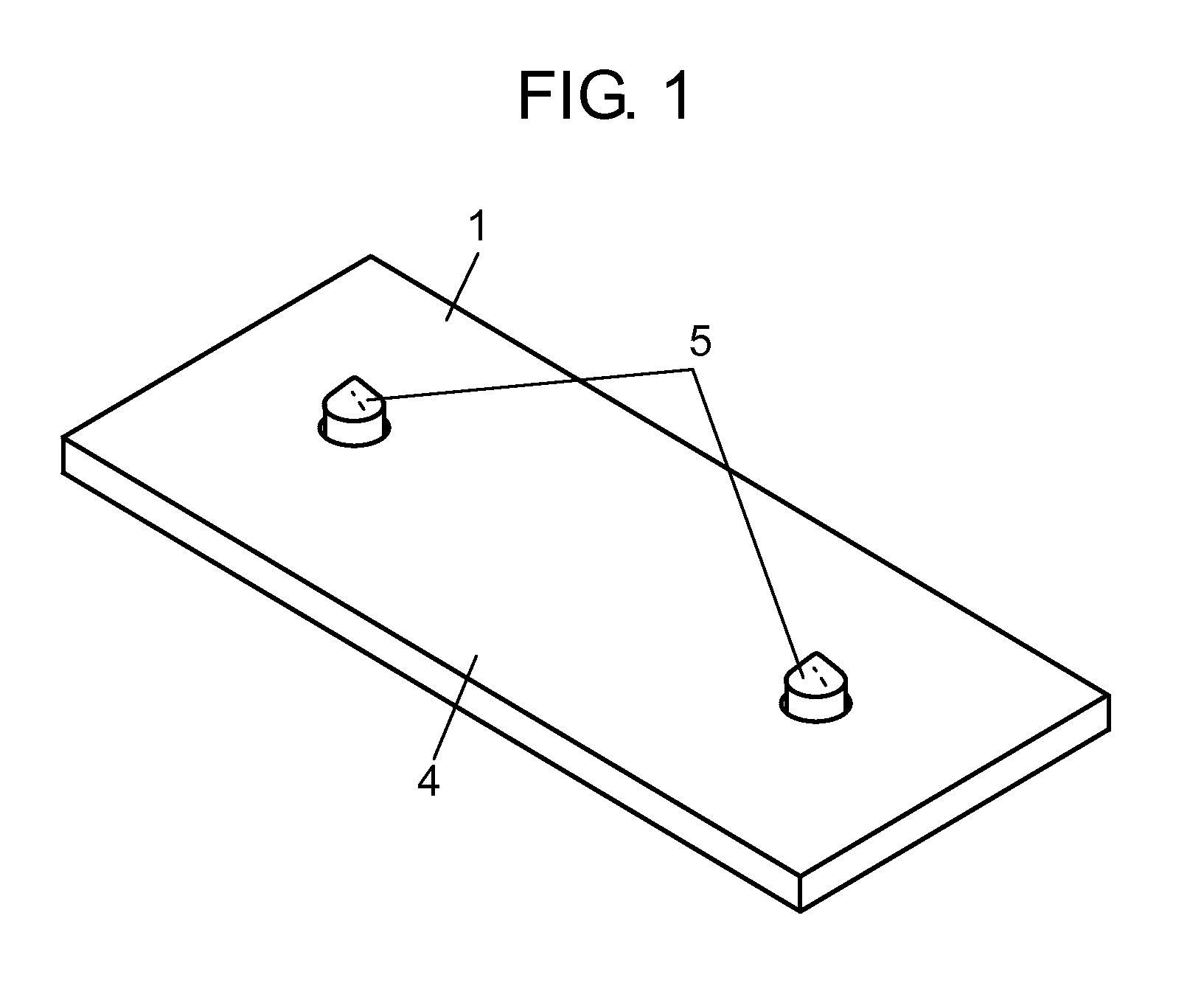
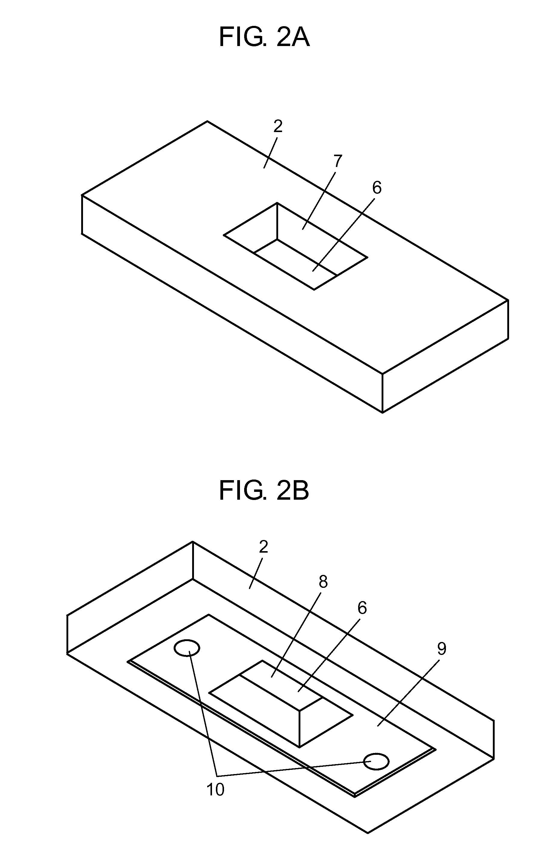
[0059]First, a structure of a mold set used in a method of manufacturing a resin molded electronic component according to Embodiment 1 of the present invention is described with reference to FIG. 1 to FIG. 3. In the following description, a capacitor is taken as an example of the electronic components. FIG. 1 is a perspective view showing an external appearance of a lower mold, FIG. 2A is a perspective view showing a top surface of a middle mold, FIG. 2B is a perspective view showing a lower surface of the middle mold, and FIG. 3 is a perspective view showing a lower surface of an upper mold. The mold set used in the method of manufacturing a resin molded capacitor in this embodiment is formed of three molds including lower mold 1, middle mold 2, and upper mold 3. By combining these three molds arranged one above the other and injecting a norbornene based resin into a cavity provided within the molds, a capacitor element laminated body is molded and an exterior packaging body is for...

embodiment 2

[0113]Next, similarly to Embodiment 1, a method of manufacturing a resin molded capacitor is described as a method of manufacturing a resin molded electronic component according to Embodiment 2 of the present invention. First, a structure of a mold set used in this manufacturing method is described with reference to FIG. 15. FIG. 15 is a cross-sectional view showing a lower mold and an upper mold.

[0114]The mold set used in the method of manufacturing a resin molded capacitor in this embodiment includes lower mold 41 and upper mold 42. Lower mold 41 is a first mold including cavity 43 with its top surface open, and upper mold 42 is a second mold that is combined with lower mold 41 on top. By combining these two molds arranged one above the other, injecting a norbornene based resin into cavity 43 of lower mold 41, and then attaching upper mold 42 to lower mold 41, an exterior packaging body of a capacitor element laminated body as a element is molded. Here, an up-down relation between...

embodiment 3

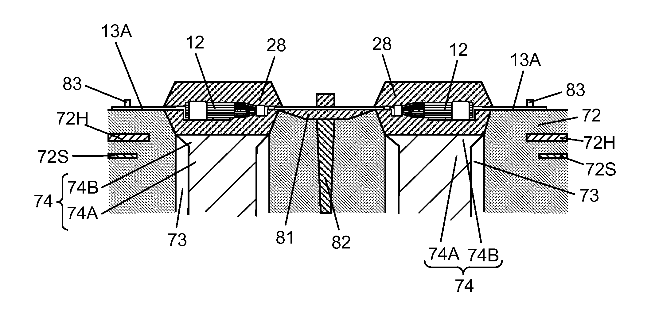
[0153]Next, similarly to Embodiment 1, a method of manufacturing a resin molded capacitor is described as a method of manufacturing a resin molded electronic component according to Embodiment 3 of the present invention. First, a structure of a mold set used in this manufacturing method is described with reference to FIG. 25. FIG. 25 is a cross-sectional view showing an upper mold and a lower mold that constitute a mold set.

[0154]The mold set used in the method of manufacturing a resin molded capacitor in this embodiment is formed of movable upper mold 71, stationary lower mold 72, and plunger 74. Lower mold 72 is disposed facing toward upper mold 71, and plunger 74 is disposed within pot 73 provided in lower mold 72.

[0155]According to the manufacturing method of this embodiment, norbornene based resin is injected and filled, using plunger 74, into a cavity defined by upper mold 71 and lower mold 72 after upper mold 71 and lower mold 72 are fastened. An exterior packaging body of a c...


PUM

PropertyMeasurementUnit
viscosityaaaaaaaaaa
temperatureaaaaaaaaaa

Abstract

A method of manufacturing a resin molded electronic component using a first mold having a cavity with an open top surface and a second mold combined with the first mold on top includes the following steps: (A) inserting a element of the electronic component and a liquid resin precursor into the cavity of the first mold, the liquid resin precursor having viscosity of 10 Pa·s or lower at 40° C.; (B) arranging the second mold such that the element and the resin precursor are sandwiched after the step (A); and (C) pressing the element and the resin precursor between the first mold and the second mold, and curing the resin precursor by heat from the second mold after the step (B). A temperature of the second mold is set to be higher than that of the first mold.

Description

[0001]This application is a U.S. National Phase Application of PCT International Application PCT / JP2010 / 004029.TECHNICAL FIELD[0002]The present invention relates to a method of manufacturing a resin molded electronic component used for various electronic devices, electrical apparatuses, industrial instruments, automobiles, and the like.BACKGROUND ART[0003]FIG. 37 is a perspective view showing a mold set used for forming an exterior packaging body of a conventional resin molded capacitor. Mold set 120 for resin-molding includes upper mold 121 and lower mold 122. Upper mold 121 is provided with gate 123 through which an uncured resin is injected. Further, upper mold 121 and lower mold 122 are provided with air vent hole 124 in mating surfaces thereof for removing air when injecting a resin.[0004]In order to mold the exterior packaging body, first, capacitor element 126 to which clasps 125 are connected is placed on lower mold 122. At this time, capacitor element 126 can be accurately ...

Claims


Application Information

Patent Timeline
Patent Type & Authority Applications(United States)
IPC IPC(8): H01G4/224H01G13/00
CPCB29C39/006B29C70/72B29C39/38B29C39/405B29C43/18B29K2023/38B29K2105/0002H01G9/012H01G9/10H01G9/15H01G13/003B29C2043/182B29C70/70B29C2043/181B29C39/10
Inventor KURITA, JUNICHITAKAHASHI, HIROSHIKURANUKI, KENJIMORIOKA, MOTOAKINAKAGAWA, KEIZOMINAKUCHI, MASASHISHIMASAKI, YUKIHIRO
Owner PANASONIC INTELLECTUAL PROPERTY MANAGEMENT CO LTD
Why Eureka
Try Eureka