Power Semiconductor Component with Plate Capacitor Structure and Edge Termination

a technology of capacitor structure and plate, applied in the direction of semiconductor devices, electrical devices, transistors, etc., can solve the problems of increasing radiofrequency interference disturbance, significant reduction of the structural volume of switched-mode power supply, and complex production of active pfc circuits, so as to slow down the switching of capacitor structures and large capacitor structures.

Inactive Publication Date: 2011-06-09
INFINEON TECH AG
View PDF4 Cites 7 Cited by
  • Summary
  • Abstract
  • Description
  • Claims
  • Application Information

AI Technical Summary

Benefits of technology

If the power semiconductor component contains a plurality of plate capacitor structures lying one beside another, it is possible to achieve a large capacitance of the capacitor structure without the electrical resistance within the field plates and edge plates slowing down the switching of the capacitor structures.

Problems solved by technology

This leads on the one hand to a significant reduction of the structural volume of the switched-mode power supply, but on the other hand also to increased radiofrequency interference disturbances.
The active PFC circuits are accordingly complicated to produce and may require a space within the switched-mode power supply, which increases the overall costs for the power supply.

Method used


Image

  • Power Semiconductor Component with Plate Capacitor Structure and Edge Termination
  • Power Semiconductor Component with Plate Capacitor Structure and Edge Termination
  • Power Semiconductor Component with Plate Capacitor Structure and Edge Termination

Examples


Embodiment Construction

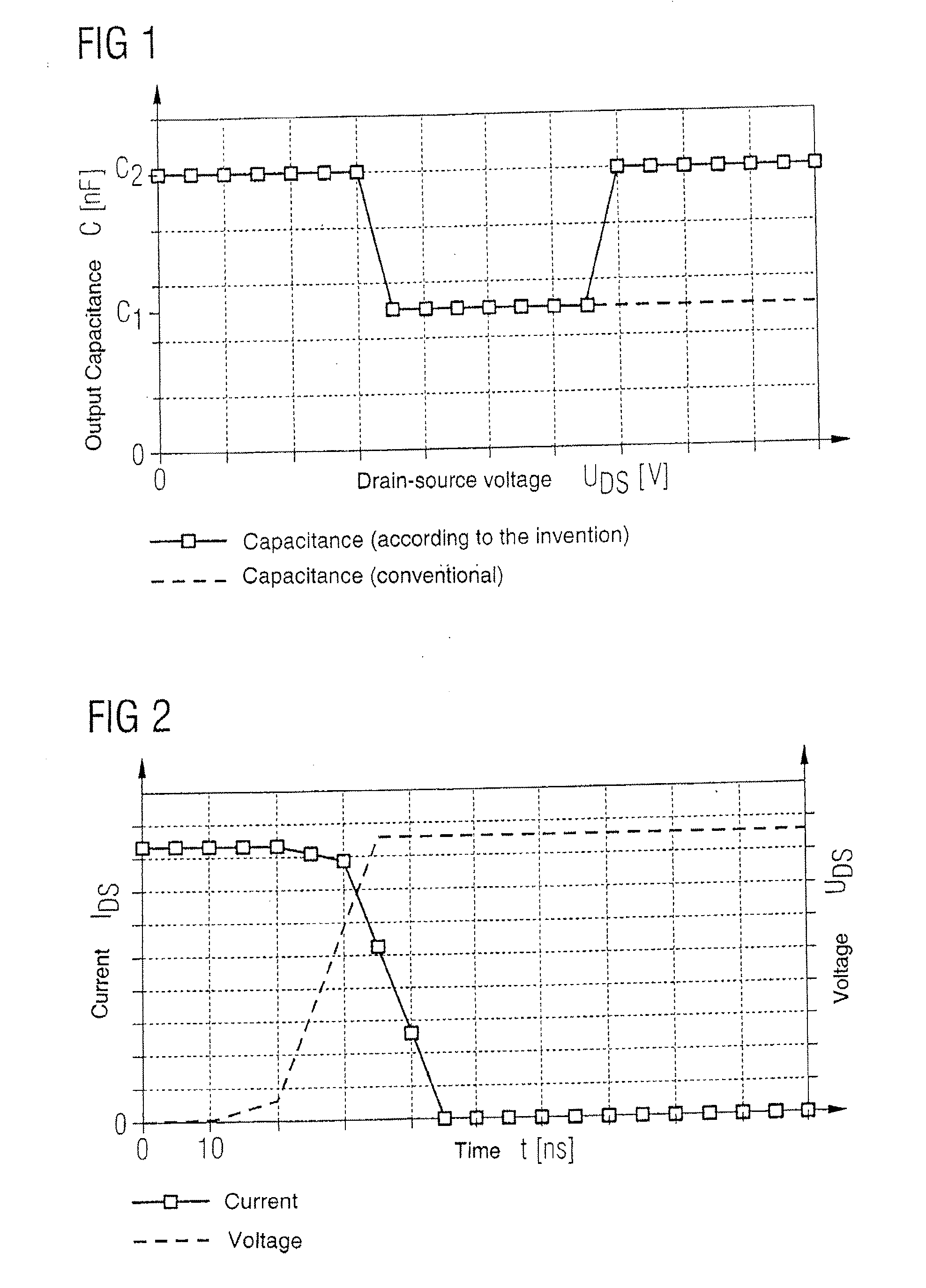
The actual and desired profiles of output capacitances of power semiconductor components are compared in FIG. 1. The area capacitance of a power semiconductor component is plotted against the drain-source voltage. The dashed line shows the profile of a conventional power semiconductor component. It remains constant at the value C1 over the entire range of the drain-source voltage.

The desired profile of a drain-source capacitance is depicted as a solid line having a “trough profile”. At low voltages it is at a value C2, then falls to the lower value C1 and remains at this value C1 before rising to the value C2 again at higher drain-source voltages.

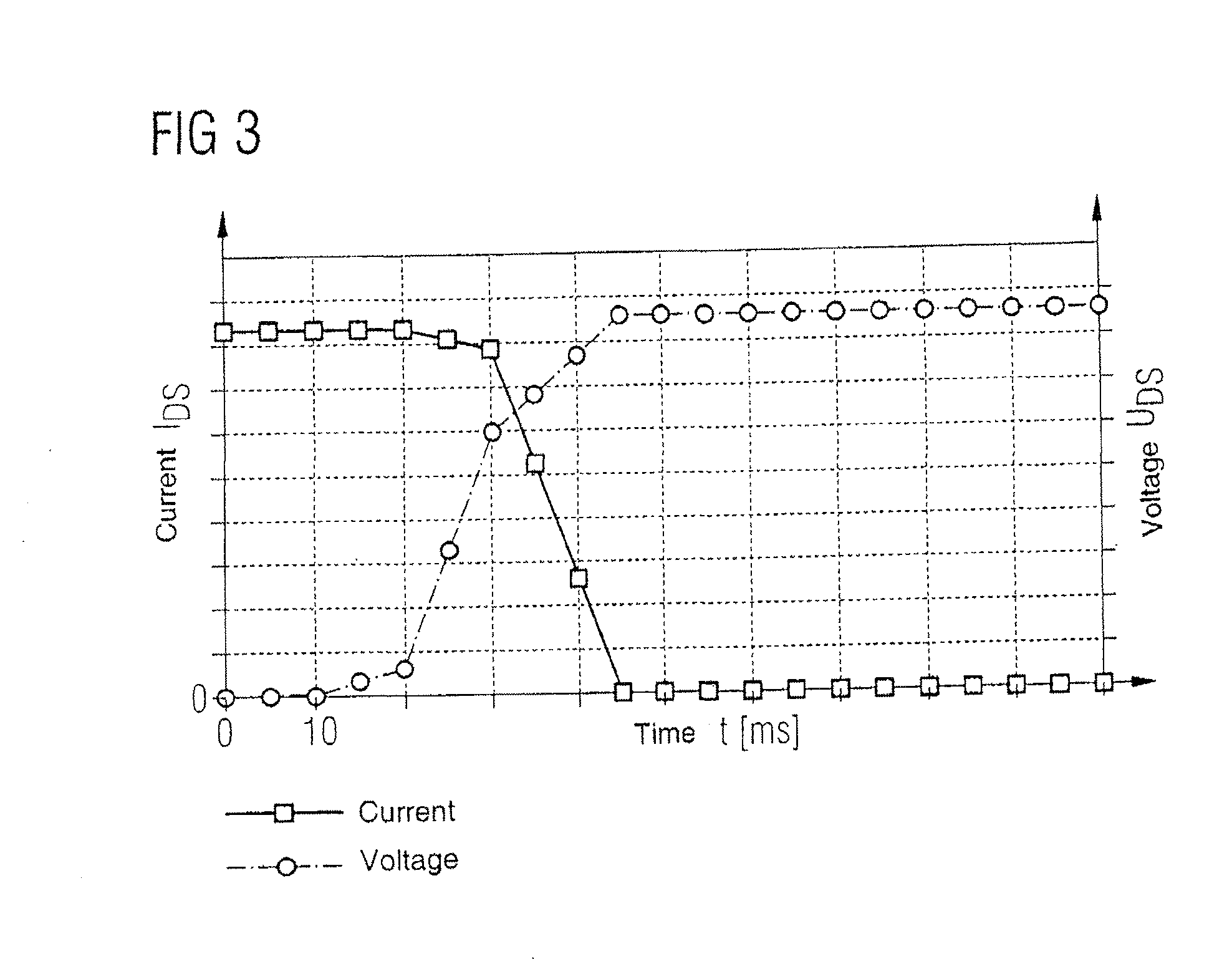
FIG. 2 shows the switch-off behavior of a power semiconductor component with a conventional output capacitance profile. A transistor is involved here. The drain-source voltage UDS and the drain-source current IDS are plotted against time. When the transistor is switched off, the drain voltage initially rises slowly before rising steeply wit...


PUM


Abstract

A semiconductor component includes a body with a drift zone, a source zone, a body zone, and a drain zone. A gate forms a MOS structure with the drift zone, with the source zone and with the body zone. An edge termination between the lateral edge and the MOS structure includes a plurality of field rings which enclose the MOS structure. The lateral edge is at the same potential as the drift zone, and the edge termination reduces voltage between the lateral edge and the source zone. A horizontally extending edge plate is disposed at the front side between the lateral edge and the edge termination. The edge plate is at the same potential as the drift zone and forms a plate capacitor structure including a field plate lying above the edge plate.

Description

TECHNICAL FIELDThe invention relates to power semiconductor components having a front side, a rear side and a lateral edge.BACKGROUNDA power semiconductor component is formed for example as a vertical power transistor with compensation pillars. Such a power semiconductor component contains a semiconductor body having at least one drift zone of the first conductivity type, a multiplicity of source zones of the first conductivity type, a drain zone of the first conductivity type and a multiplicity of body zones of the second conductivity type.Such a vertical power transistor furthermore contains at least one gate which forms a MOS structure with a drift zone, a source zone and with a body zone. It contains compensation pillars of the second conductivity type which are in electrical contact with the source zones and which project into the drift zone from above. An edge termination is situated between the edge and the MOS structure. The edge is at the same potential as the drift zone, s...

Claims


Application Information

Patent Timeline
Patent Type & Authority Applications(United States)
IPC IPC(8): H01L29/78
CPCH01L29/0619H01L29/0634H01L29/1095H01L29/7823H01L29/7803H01L29/7811H01L29/7817H01L29/402
Inventor WAHL, UWEWILLMEROTH, ARMIN
Owner INFINEON TECH AG
Why Eureka
Try Eureka