Semiconductor memory device and method for driving the same

a memory device and semiconductor technology, applied in semiconductor devices, digital storage, instruments, etc., can solve the problems of less potential change, less reading accuracy, and more complex data reading when compared to data writing, and achieve the effect of sufficient capacitan

Inactive Publication Date: 2012-03-29
SEMICON ENERGY LAB CO LTD
View PDF5 Cites 42 Cited by
  • Summary
  • Abstract
  • Description
  • Claims
  • Application Information

AI Technical Summary

Benefits of technology

[0043]Here, the sub bit line SBL_n_m is sufficiently short and its parasitic capacitance is thus sufficiently small as compared to the parasitic capacitance of the bit line MBL_m. Thus, even when the capacitance of the capacitor of the memory cell is small, a signal can be amplified by the amplifier circuit AMP_n_m without a malfunction, and the amplified signal can be output to the bit line MBL_m.
[0044]It is needless to say that the amplified signal includes noise that is large when measured in an extremely short time; however, an adverse effect of the noise can be cancelled in a process of accumulating electric charge in the bit line MBL_m whose capacitance is sufficiently large. That is, a memory device having a function equivalent to a conventional DRAM and a smaller capacitor than the conventional DRAM can be manufactured.

Problems solved by technology

Data reading is more complex when compared to data writing.
A problem in the above operation is reading accuracy.
As the capacitance of the capacitor becomes relatively smaller than the parasitic capacitance of the bit line MBL, potential change becomes smaller; thus, errors easily occur at the time of reading.
Although the size of a memory cell tends to be reduced as miniaturization proceeds, the capacitance of a capacitor of the memory cell cannot be reduced because a predetermined ratio of the capacitance of the capacitor to the parasitic capacitance of a bit line needs to be kept in the above-described manner.
That is, an extremely long and narrow structure body whose depth or height is 2 μm or more needs to be formed in a limited area, which is difficult to realize with high yield.
However, the present inventor found that the semiconductor memory device disclosed in Patent Document 1 cannot stably operate and a malfunction easily occurs when capacitance (including parasitic capacitance), examples of which are the capacitance of a sub bit line, the capacitance of a capacitor connected to the sub bit line, and the capacitance of input of a flip-flop circuit, is 1 fF or less.
Such a malfunction is mainly caused by noise.
Thus, potential change of the bit line is limited even with very large noise.
However, when a flip-flop circuit or the like is incorporated, an adverse effect of noise comes to the surface.
Thus, the DRAM disclosed in Patent Document 1 cannot be used in the case where the capacitance of a capacitor is very small.
However, when the capacitance of the capacitor is ten or less times as large as the capacitance of the input of the flip-flop circuit, the flip-flop circuit is influenced by its gate capacitance and operation becomes unstable.
Specifically, in a condition where the capacitance of the capacitor is two or less times as large as the capacitance of the input of the flip-flop circuit, it is almost impossible to control the flip-flop circuit in accordance with the capacitance of the capacitor.

Method used


Image

  • Semiconductor memory device and method for driving the same
  • Semiconductor memory device and method for driving the same
  • Semiconductor memory device and method for driving the same

Examples


embodiment 1

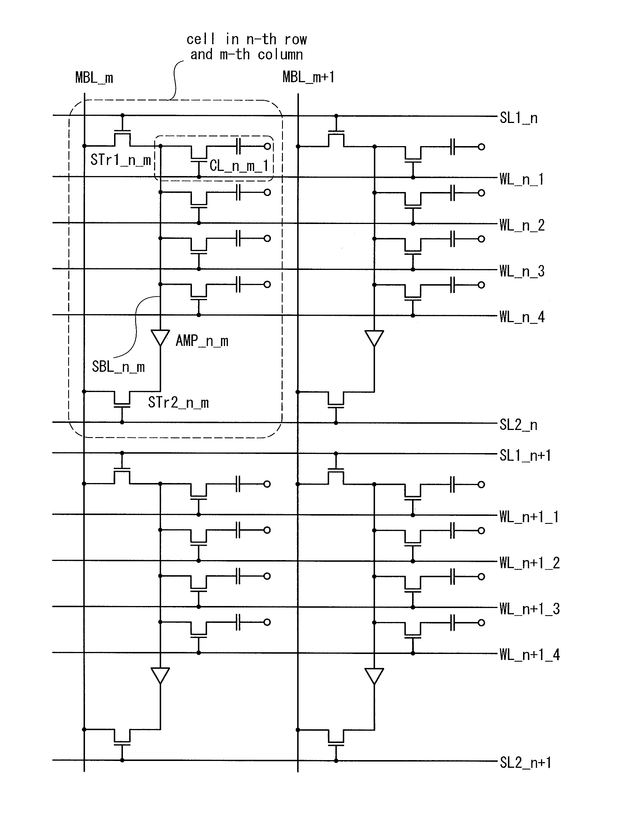
[0065]In this embodiment, a semiconductor memory device illustrated in FIG. 1 and an example of its operation are described with reference to FIGS. 2A to 2 C, FIGS. 3A and 3B, FIGS. 4A to 4C, and FIGS. 5A to 5C. Note that specific values are given below as potentials for the purpose of aid for understanding the technical idea of the present invention. Needless to say, such values are changed in accordance with various characteristics of a transistor, a capacitor, or the like, or for convenience of the practitioner. Further, the semiconductor memory device described in this embodiment can write or read data using a method other than a method described below.

[0066]The semiconductor memory device illustrated in FIG. 1 includes word lines WL, bit lines MBL intersecting with the word lines, first selection lines SL1 and second selection lines SL2 which are parallel to the word lines WL, and a plurality of cells. Each cell includes a first selection transistor STr1, a second selection tra...

embodiment 2

[0108]An example of a method for manufacturing a semiconductor memory device according to part of the technical idea of the present invention is described with reference to FIGS. 6A to 6C, FIGS. 7A and 7B, and FIG. 8. Note that FIGS. 6A to 6C, FIGS. 7A and 7B, and FIG. 8 show cross sections of the semiconductor memory device following a process for manufacturing the semiconductor memory device; the cross sections do not show the cross-sections of a specific part.

[0109]First, by a known semiconductor processing technique, an element separation insulator 102, a p-well 101P, and an n-well 101N are formed over one surface of a substrate 101 which is formed of a single crystal semiconductor such as silicon, gallium arsenide, gallium phosphide, silicon carbide, germanium, or germanium silicide. Further, a gate 104N of an n-channel transistor, an n-type impurity region 103N, a gate 104P of a p-channel transistor, and a p-type impurity region 103P are formed. In addition, a first interlayer...

embodiment 3

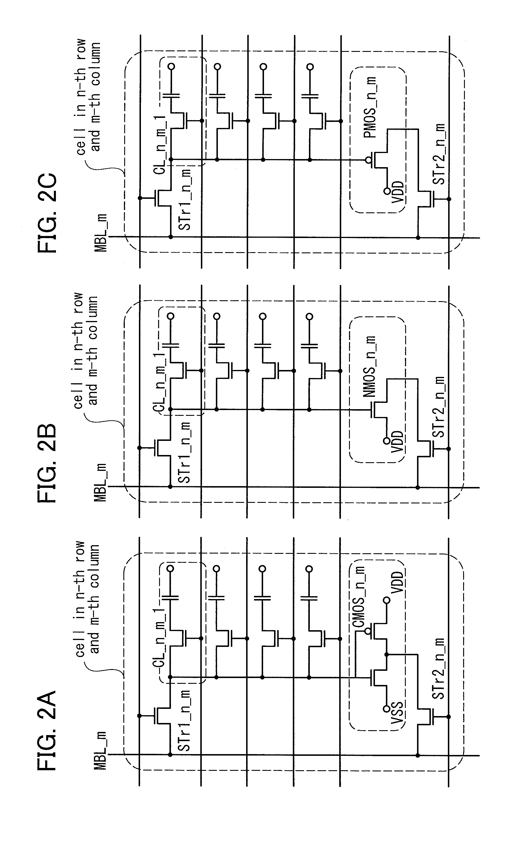
[0124]In this embodiment, a semiconductor memory device illustrated in FIG. 10 and an operation example thereof are described. FIG. 10 shows the cell in the n-th row and the m-th column, the cell in the n-th row and the (m+1)-th column, and part of a driver circuit in the m-th column and the (m+1)-th column which are included in the semiconductor memory device.

[0125]The cell of the semiconductor memory device of this embodiment includes the first selection transistor STr1, the second selection transistor STr2, a plurality of memory cells, an amplifier circuit, and the sub bit line SBL. Although the n-channel transistor NMOS is included as the amplifier circuit in the semiconductor memory device illustrated in FIG. 10, a p-channel transistor may be alternatively used.

[0126]The drain of the first selection transistor STr1_n_m and the drain of the first selection transistor STr1_n_m+1 are respectively connected to the bit line MBL_m and the bit line MBL_m+1; the source of the first sel...


PUM


Abstract

In a conventional DRAM, when the capacitance of a capacitor is reduced, an error of reading data easily occurs. A plurality of cells are connected to one bit line MBL_m. Each cell includes a sub bit line SBL_n_m and 4 to 64 memory cells (a memory cell CL_n_m1 or the like). Further, each cell includes selection transistors STr1_n_m and STr2_n_m and an amplifier circuit AMP_n_m that is a complementary inverter or the like is connected to the selection transistor STr2_n_m. Since parasitic capacitance of the sub bit line SBL_n_m is sufficiently small, potential change due to electric charge in a capacitor of each memory cell can be amplified by the amplifier circuit AMP_n_m without an error, and can be output to the bit line.

Description

BACKGROUND OF THE INVENTION[0001]1. Field of the Invention[0002]The present invention relates to a memory device using a semiconductor.[0003]2. Description of the Related Art[0004]Terms used in this specification will be briefly explained. First, when one of a source and a drain of a transistor is called a drain, the other is called a source in this specification. That is, they are not distinguished depending on the potential level. Therefore, a portion called a source in this specification can be alternatively referred to as a drain.[0005]Further, even when it is written in this specification that “to be connected”, there is a case in which no physical connection is made in an actual circuit and a wiring is only extended. For example, in an insulated-gate field-effect transistor (hereinafter simply referred to as a transistor) circuit, there is a case in which one wiring serves as gates of a plurality of transistors. In this case, one wiring may have a plurality of branches to gate...

Claims


Application Information

Patent Timeline
Patent Type & Authority Applications(United States)
IPC IPC(8): G11C11/24
CPCG11C8/14G11C11/404G11C11/4076G11C11/4087H01L27/0207H01L27/0688G11C11/4094H01L27/10873H01L27/10894H01L27/10897H01L27/1207H01L27/1225G11C11/4085H01L27/10805G11C7/02G11C11/4097G11C11/4091G11C11/4096H01L27/124H01L27/1255H10B12/312H10B12/30H10B12/05H10B12/09H10B12/50H10B99/00H10B12/00H01L27/092
Inventor TAKEMURA, YASUHIKO
Owner SEMICON ENERGY LAB CO LTD
Why Eureka
Try Eureka