Liquid crystal display device

a liquid crystal display and display device technology, applied in semiconductor devices, instruments, electrical devices, etc., can solve the problems of inability to increase the holding capacitance, damage to the source electrode sdb>2/b>, and patent document 1 fails to describe a material of the film, etc., to achieve the effect of reducing the damage, reducing the damage, and reducing the cost of production

Active Publication Date: 2007-12-27
PANASONIC LIQUID CRYSTAL DISPLAY CO LTD +1
View PDF4 Cites 46 Cited by
  • Summary
  • Abstract
  • Description
  • Claims
  • Application Information

AI Technical Summary

Benefits of technology

[0041]According to the present invention, it is possible to form a holding capacitance which exhibits a large capacitance.
[0042]Further, the present invention can prevent damages from being applied to the source electrode.
[0043]Further, according to the present invention, the process can be simplified.
[0044]Further, according to the present invention, it is possible to ensure the electric connection in the contact hole.

Problems solved by technology

However, in the liquid crystal display device shown in FIG. 7, when the coated insulation film is used as the interlayer insulation film IN3A, the interlayer insulation film IN3A exhibits a dielectric constant which is not so high thus giving rise to a drawback that the holding capacitance cannot be increased.
Further, although patent document 1 describes a technique which forms the interlayer insulation film IN3A by the CVD method in place of the coated insulation film, patent document 1 fails to describe a material of the film.
Accordingly, there exists a possibility that the source electrode SD2 is damaged by etching which is performed for patterning the reflection film RAL using an etchant or an etching gas.

Method used


Image

  • Liquid crystal display device
  • Liquid crystal display device
  • Liquid crystal display device

Examples


embodiment 1

[0053]In an embodiment 1, the explanation is made with respect to one example in which the present invention is applied to an IPS liquid crystal display device.

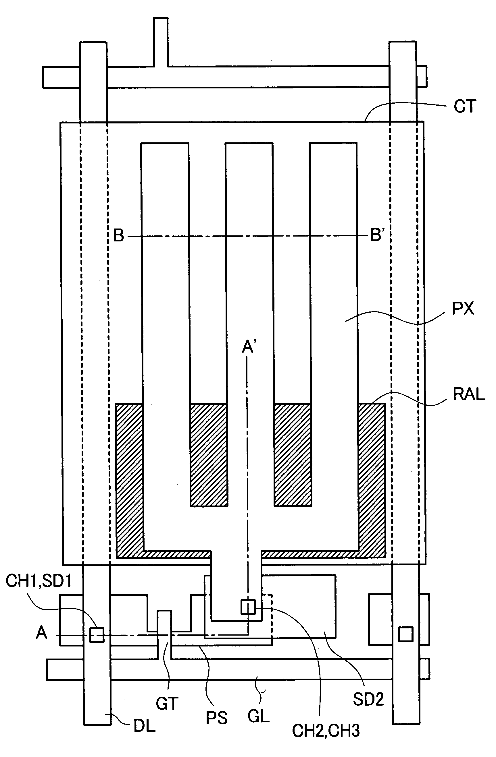
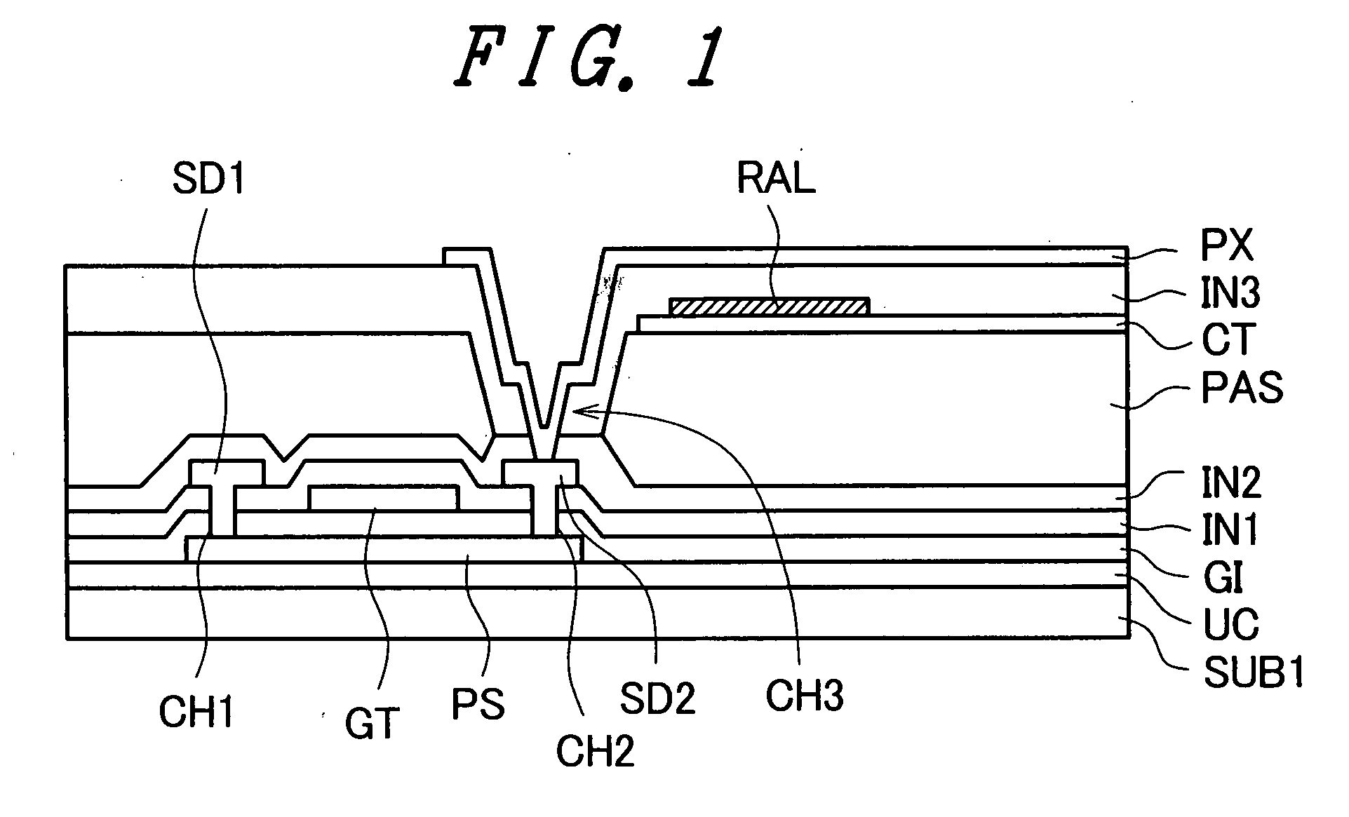
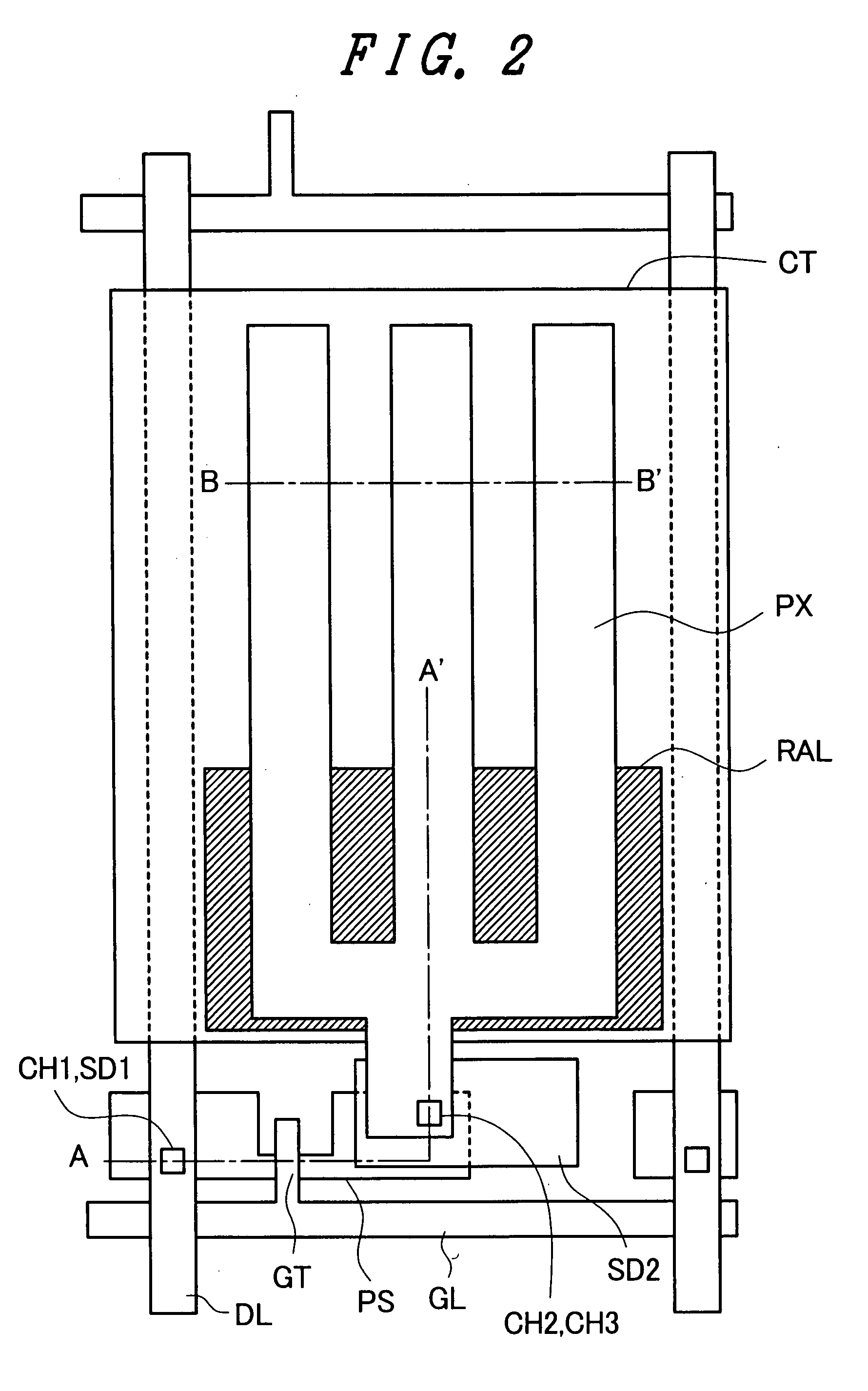
[0054]FIG. 1 is a view for explaining a liquid crystal display device of the embodiment 1 of the present invention and also is a cross-sectional view taken along a line A-A′ in FIG. 2. FIG. 2 is a plan view for explaining the liquid crystal display device of the embodiment 1 of the present invention. FIG. 3 is a view for explaining the liquid crystal display device of the embodiment 1 of the present invention and also is a cross-sectional view taken along a line B-B′ in FIG. 2.

[0055]As shown in FIG. 1 to FIG. 3, liquid crystal LC is sandwiched between a transparent insulation substrate (first substrate) SUB1 made of a glass or the like and a transparent insulation counter substrate (second substrate) SUB2 made of a glass or the like.

[0056]The liquid crystal display device according to the present invention is an active matrix...

embodiment 2

[0083]In the embodiment 2, one example in which the formation of a surface unevenness to perform a diffusion reflection is applied to the constitution of the embodiment 1 is explained. FIG. 5 is a view for explaining the embodiment 2 of the liquid crystal display device according to the present invention, and also is a view corresponding to FIG. 1. Here, in this embodiment and succeeding embodiments which follow the embodiment 2, points makes these embodiments different from the embodiment 1 are mainly explained and the explanation of contents common with the contents of the embodiment 1 is omitted.

[0084]The constitution which makes the embodiment 2 different from the constitution of the embodiment 1 lies in that the surface unevenness (projections PJ) is formed on a portion of the organic insulation film PAS corresponding to the reflection film RAL by making use of a halftone exposure, for example, and the reflection film RAL has an uneven surface shape by reflecting the surface un...

embodiment 3

[0087]The embodiment 3 describes a modification of a shape of the contact hole CH3 of the present invention.

[0088]FIG. 6A to FIG. 6C are views for explaining the embodiment 3 of the present invention, and also are cross-sectional views showing the contact hole portion in an enlarged manner.

[0089]As shown in FIG. 6A and FIG. 6B, in the contact hole CH3, it is desirable that an organic insulation film PAS is not exposed from an interlayer insulation film IN3. That is, in the contact hole CH3, it is desirable that a lower surface of the interlayer insulation film IN3 is brought into contact with an upper surface of an interlayer insulation film IN2 over the whole circumference.

[0090]As shown in FIG. 6C, at an exposed portion EX where the organic insulation film PAS is exposed from the interlayer insulation film IN3, a pixel electrode PX formed on the interlayer insulation film IN3 may possess a high resistance or is liable to be easily disconnected. Such an exposed portion PX is formed...


PUM


Abstract

The present invention provides a liquid crystal display device having a large holding capacitance in the inside of a pixel. A liquid crystal display device includes a first substrate, a second substrate arranged to face the first substrate in an opposed manner, and liquid crystal sandwiched between the first substrate and the second substrate. The first substrate includes a video signal line, a pixel electrode, a thin film transistor having a first electrode thereof connected to the video signal line and a second electrode thereof connected to the pixel electrode, a first silicon nitride film formed above the second electrode, an organic insulation film formed above the first silicon nitride film, a capacitance electrode formed above the organic insulation film, and a second silicon nitride film formed above the capacitance electrode and below the pixel electrode. The second silicon nitride film is a film which is formed at a temperature lower than a forming temperature of the first silicon nitride film. The first silicon nitride film and the second silicon nitride film form a contact hole therein by etching both of the first silicon nitride film and the second silicon nitride film collectively by dry etching. The second electrode and the pixel electrode are connected to each other via the contact hole. A potential different from a potential applied to the pixel electrode is applied to the capacitance electrode, and a holding capacitance is formed by the pixel electrode, the second silicon nitride film and the capacitance electrode.

Description

[0001]The present application claims priority from Japanese application JP2006-160428 filed on Jun. 9, 2006, the content of which is hereby incorporated by reference into this application.BACKGROUND OF THE INVENTION[0002]1. Field of the Invention[0003]The present invention relates to a liquid crystal display device, and more particularly to a technique which is effectively applicable to a liquid crystal display device which includes a silicon nitride film.[0004]2. Description of Related Art[0005]An active matrix liquid crystal display device forms a holding capacitance in the inside of a pixel for holding a video signal written in the pixel for a relatively long time.[0006]The inventors of the present invention filed a patent application (see following patent document 1) on one method for forming such a holding capacitance.[0007]FIG. 7 is a cross-sectional view of an essential part showing one example of the holding capacitance described in patent document 1.[0008]As shown in FIG. 7...

Claims


Application Information

Patent Timeline
Patent Type & Authority Applications(United States)
IPC IPC(8): H01L21/00
CPCG02F1/133504G02F1/133555G02F1/136213G02F1/134363G02F1/136227G02F1/13685G02F1/1368G02F1/133345G02F1/133305H01L27/124H01L27/1248H01L29/78675
Inventor TANABE, HIDEOTAKABATAKE, MASARUKANEKO, TOSHIKIHASEGAWA, ATSUSHISEHATA, HIROKO
Owner PANASONIC LIQUID CRYSTAL DISPLAY CO LTD
Why Eureka
Try Eureka