Capacitive pressure sensor and method therefor

a technology of capacitance sensor and capacitance sensor, which is applied in the direction of fluid pressure measurement, electrolytic capacitor, instruments, etc., can solve the problems of inability to achieve the effect of reducing increasing the size of the sensor, and being susceptible to parasitic capacitan

Active Publication Date: 2008-03-06
EVIGIA SYST
View PDF6 Cites 46 Cited by
  • Summary
  • Abstract
  • Description
  • Claims
  • Application Information

AI Technical Summary

Benefits of technology

[0006] The present invention provides a method of fabricating a MEMS capacitive pressure sensor, and the resulting pressure sensor. The sensor has a pressure-sensing diaphragm that is mechanical coupled but electrical isolated from a mechanical capacitor that generates the output of the sensor. Because the diaphragm is electrically decoupled from the capacitor, the diaphr...

Problems solved by technology

However, capacitive pressure sensors are susceptible to parasitic capacitances and therefore need to be integrated with interface circuitry.
In addition, their dynamic range is limited unless closed-loop operation is utilized and high pressure resolution can be achieved with the sensor structure.
However, increased sensor size is often undesirable or not practical and increased deflection is associated with nonlinearity in the output that requires additional compensation circuitry, with the further disadvantage of consuming more ...

Method used


Image

  • Capacitive pressure sensor and method therefor
  • Capacitive pressure sensor and method therefor
  • Capacitive pressure sensor and method therefor

Examples


Embodiment Construction

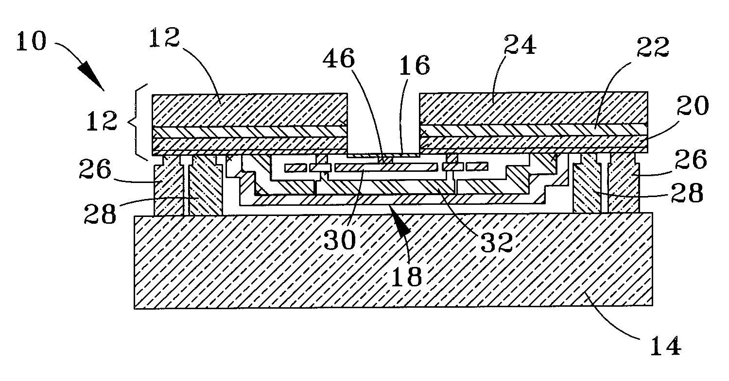
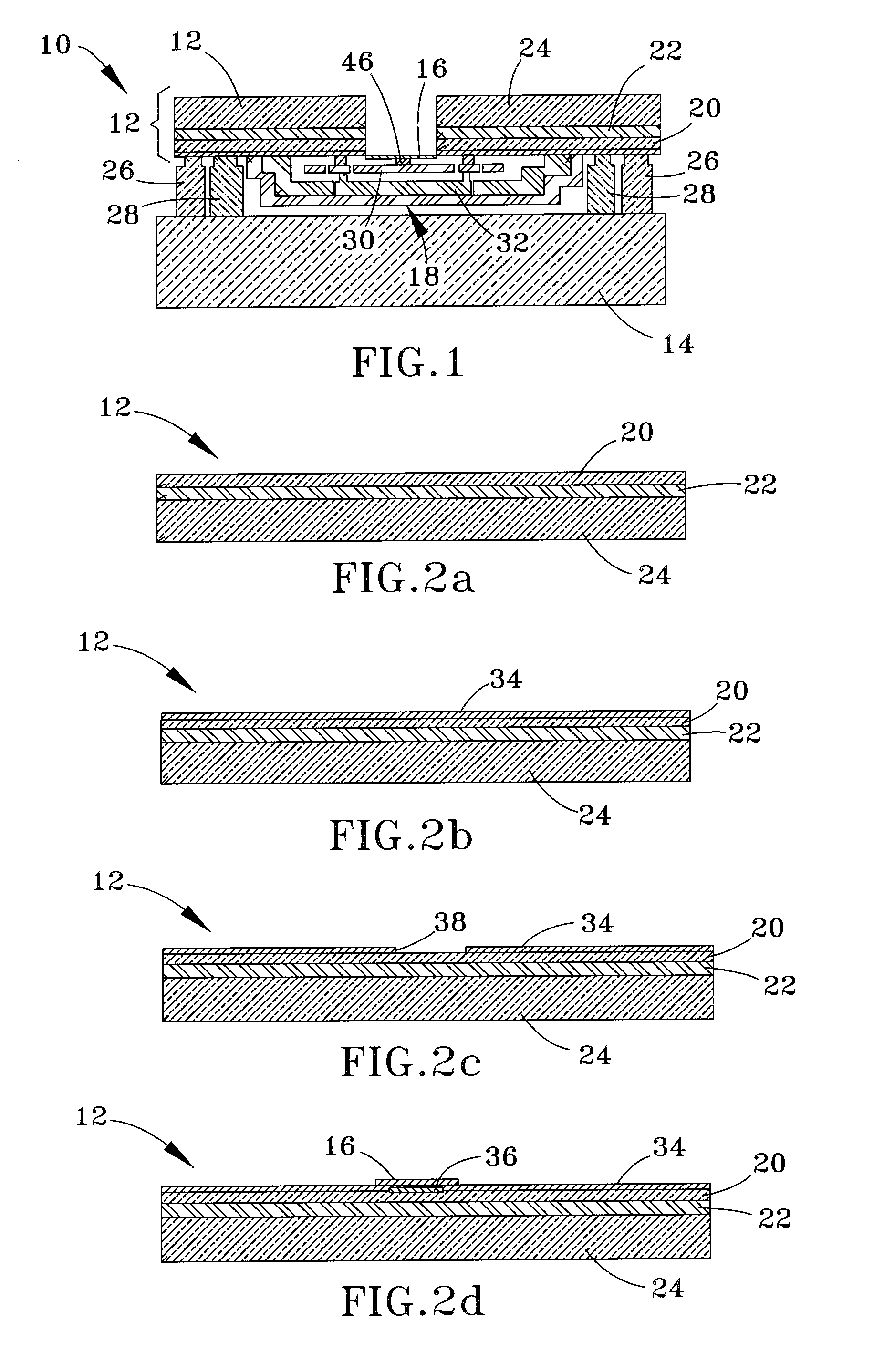
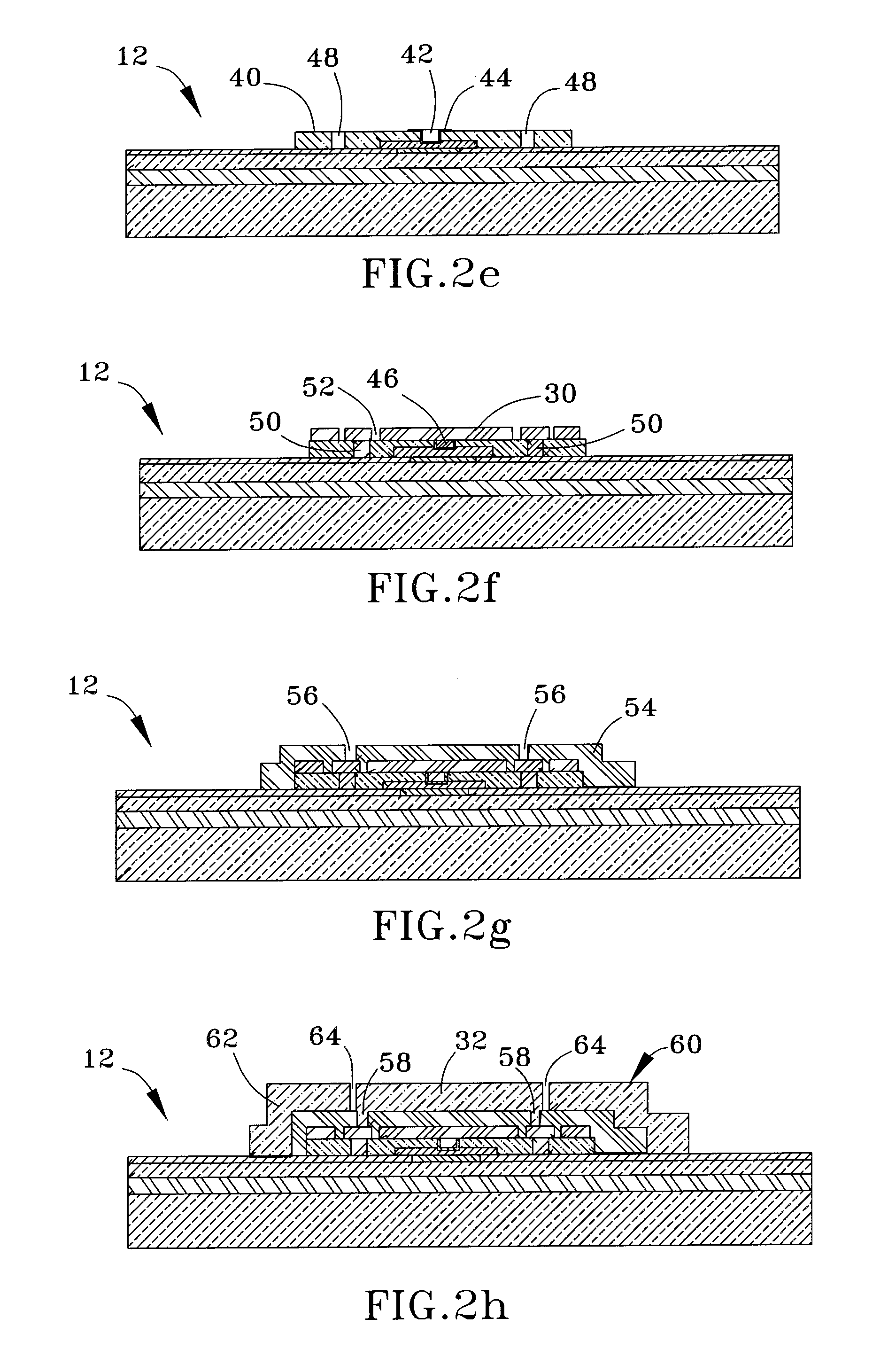
[0016] Illustrated in FIG. 1 is a capacitive pressure sensor 10 within the scope of the present invention, while FIGS. 2a through 2n represent suitable steps for its fabrication. The drawings are drawn for purposes of clarity when viewed in combination with the following description, and therefore are not necessarily to scale. It should also be noted that terms such as “upper,”“lower,”“topside,” and “backside” are in reference to the sensor 10 as shown in the Figures, and are not limitations to the sensor 10 or its use.

[0017] In FIG. 1, an SOI wafer 12 carrying a pressure-sensing diaphragm 16 and a mechanical capacitor 18 are shown bonded to a second wafer 14 carrying interface circuitry (not shown) for the capacitor 18. According to a preferred implementation of the invention, the wafer 14 is a CMOS wafer, and will be referred to as such in the following discussion. As is conventional, the SOI wafer 12 is shown as including an electrically-conductive (e.g., doped silicon) device l...


PUM

PropertyMeasurementUnit
Electrical conductoraaaaaaaaaa

Abstract

A capacitive pressure sensor and method for its fabrication. The sensor is fabricated from first and second wafers to have a mechanical capacitor comprising a fixed electrode and a moving electrode defined by a conductive plate. The sensor further has a diaphragm on a surface of the first wafer that is mechanically coupled but electrically insulated from the conductive plate. A conductive layer on the surface of the first wafer is spaced apart from the conductive plate to define the fixed electrode. The second wafer is bonded to the first wafer and carries interface circuitry for the sensor, including the conductive plate and the fixed electrode which are between the first and second wafers and electrically connected to the interface circuitry. At least an opening is present in the first wafer and its first conductive layer by which the diaphragm is released and exposed to an environment surrounding the sensor.

Description

CROSS REFERENCE TO RELATED APPLICATIONS [0001] This application claims the benefit of U.S. Provisional Application No. 60 / 841,428, filed Aug. 31, 2006, the contents of which are incorporated herein by reference.BACKGROUND OF THE INVENTION [0002] The present invention generally relates to MEMS (micro-electro-mechanical system) devices. More particularly, the invention relates to a capacitive pressure sensor capable of exhibiting high sensitivity in a small die size, due in part to a pressure-sensing diaphragm mechanically coupled but electrically insulated from a mechanical capacitor that generates the electrical output of the sensor. [0003] As well known in the art, capacitive pressure sensors employ a diaphragm that deflects in response to pressure, so that an electrode carried or defined by the diaphragm moves relative to a fixed (stationary) electrode with which the diaphragm defines a mechanical capacitor. Capacitive pressure sensors can be configured for measuring absolute, dif...

Claims


Application Information

Patent Timeline
IPC IPC(8): G01L9/12H01G9/00
CPCB81B2201/0264B81C1/00158Y10T29/417G01L9/0073H01G5/16G01L9/0042
Inventor GOGOI, BISHNU PRASANNAYAZDI, NAVID
Owner EVIGIA SYST
Why Eureka
Try Eureka