Process of fabricating high resistance CMOS resistor

Active Publication Date: 2005-10-13
SEMICON COMPONENTS IND LLC
View PDF11 Cites 1 Cited by
  • Summary
  • Abstract
  • Description
  • Claims
  • Application Information

AI Technical Summary

Benefits of technology

[0009] The present invention provides a process of fabricating a high resistance CMOS resistor with a relatively small die-size

Problems solved by technology

Though these resistors have satisfactory resistor characteristics, their resistance is generally limited to 1 kΩ-5 kΩ per square.
However, neither of these alternatives is desirable because they both in

Method used


Image

  • Process of fabricating high resistance CMOS resistor
  • Process of fabricating high resistance CMOS resistor
  • Process of fabricating high resistance CMOS resistor

Examples


Embodiment Construction

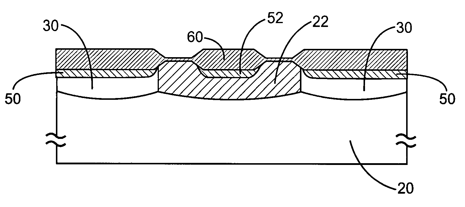
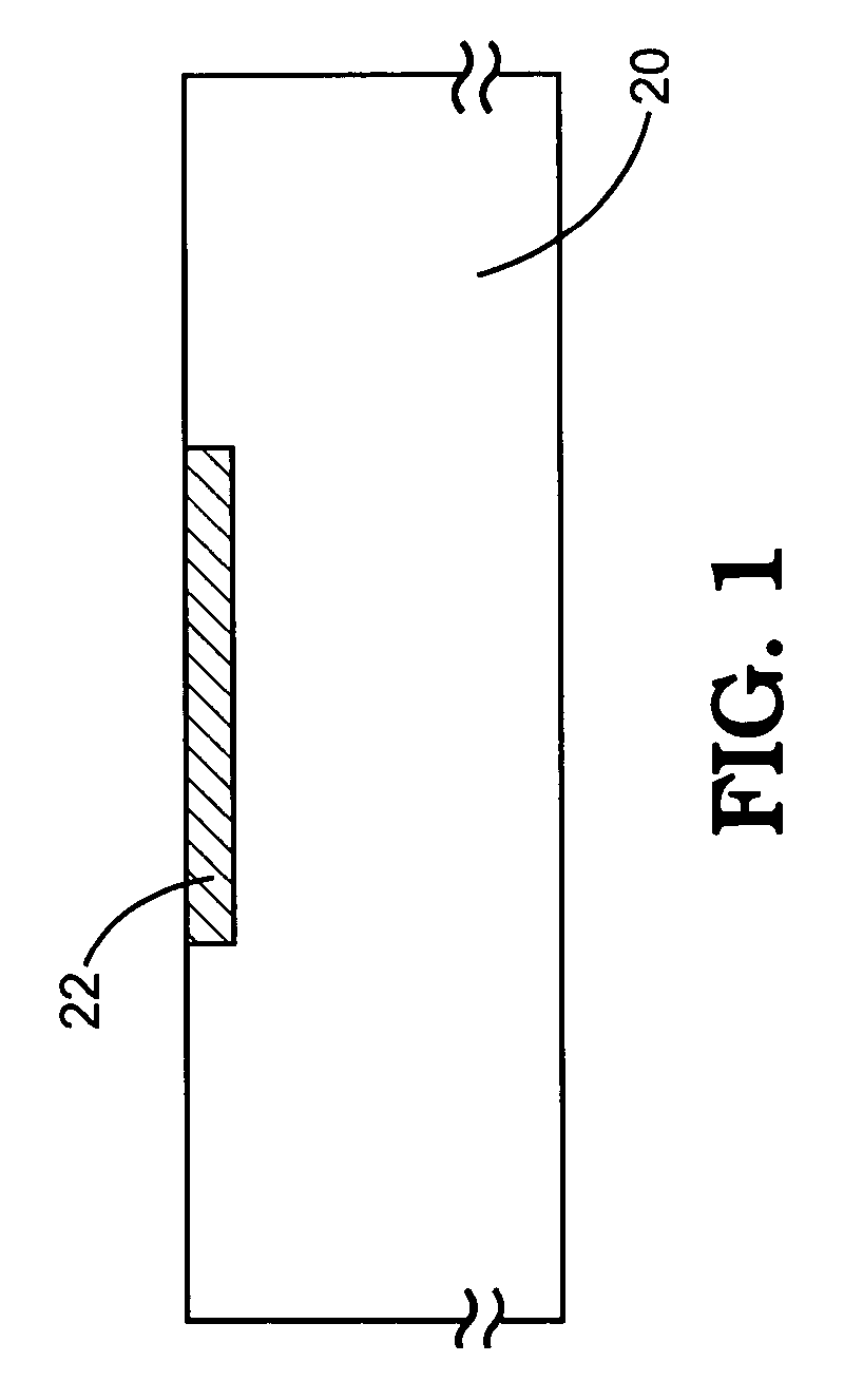
[0024] Referring now to the drawings wherein the contents are for purposes of illustrating the preferred embodiment of the invention only and not for purposes of limiting the same. Referring to FIG. 1, phosphorus ions are implanted in a p-type silicon substrate 20 to form an n-well 22. The p-type silicon substrate 20 is doped with boron ions to achieve a resistance of 8Ω-12Ω per cm. The n-well 22 can be formed via well-known photolithography, etching and implantation process as follows. A photoresist layer is formed over the p-type silicon substrate 20. Next, the photoresist layer is exposed using a mask to expose predetermined portions of the photoresist layers. Next, the exposed photoresist is etched to remove the predetermined portions of the p-type silicon substrate 20. Next, an ion implementation is then carried out using an energy level of 100 KeV using phosphorus ions with a dosage level ranging from 6×10¹² to 9×10¹² ions / cm2.

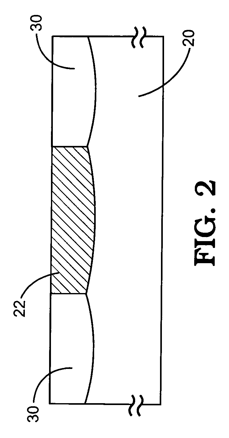
[0025] Next, as FIG. 2 shows, boron ions are impl...


PUM


Abstract

A process of forming a high resistance CMOS resistor with a relatively small die size is provided. According to an aspect of the present invention, the process of fabricating a high resistance resistor is a standard CMOS process that does not require any additional masking. An n-well is firstly formed in a p-type silicon substrate. A nitride film is then deposited and patterned to form a patterned mask layer. The patterned mask layer serves as a mask. A p-field region is formed in the n-well to form a CMOS resistor. The CMOS resistor according to the present invention has a resistance of 10 kΩ-20 kΩ per square.

Description

BACKGROUND OF THE INVENTION [0001] 1. Field of the Invention [0002] The present invention relates to a semiconductor manufacturing process, and more specifically to a process of fabricating a high resistance CMOS resistor. [0003] 2. Description of Related Art [0004] Many common circuits manufactured using CMOS process require resistor elements. In the area of analog circuits, resistor elements having high-resistance values (100 kΩ-500 kΩ) are sometimes desired. The demand for such resistors is especially common in the field of power-relative analog circuits. [0005] In one common application, many power-relative analog circuits include voltage dividers constructed from a pair of CMOS resistors. Such voltage dividers provide reference voltages that are stepped down from a supply voltage. The higher the resistance of the resistors is, the less standby power will be consumed. [0006] Currently, most widely used CMOS resistors are either junction resistors or film resistors. Common juncti...

Claims


Application Information

Patent Timeline
IPC IPC(8): H01L21/02H01L21/8238H01L27/06H01L27/08
CPCH01L27/0629H01L28/20H01L27/0802
Inventor HUANG, CHIH-FENGCHIEN, TUO-HSIN
Owner SEMICON COMPONENTS IND LLC
Why Eureka
Try Eureka