

Display device
a display device and display technology, applied in the field of display devices, can solve the problems of increasing manufacturing costs, and achieve the effect of increasing manufacturing costs and increasing the number of manufacturing processes
- Summary
- Abstract
- Description
- Claims
- Application Information
AI Technical Summary
Benefits of technology
Problems solved by technology
Method used
Image

Examples
first embodiment
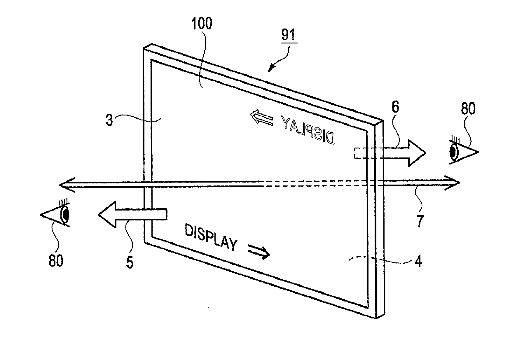
[0038]FIG. 1 is a perspective view illustrating an outline of an organic EL device 91 relating to the first embodiment of the invention and organic EL devices relating to each of the other embodiments described later. The organic EL device 91 has a display region 100 where both the upper surface and lower surface substantially overlap in a plan view. A surface seen with an eye 80 on a left side is an upper surface 3 which is a first surface, and a surface seen with an eye 80 on a right side is a lower surface 4 which is a second surface.
[0039]From the upper surface 3, a first display light 5 is irradiated, and from the lower surface 4, a second display light 6, which is different display light from the first display light 5, is irradiated. “Different display light” refers to light forming a different image. Accordingly, the organic EL device 91 can display images which are each different to two viewers who are positioned to be facing with the organic EL device 91 therebetween. Here,...
second embodiment
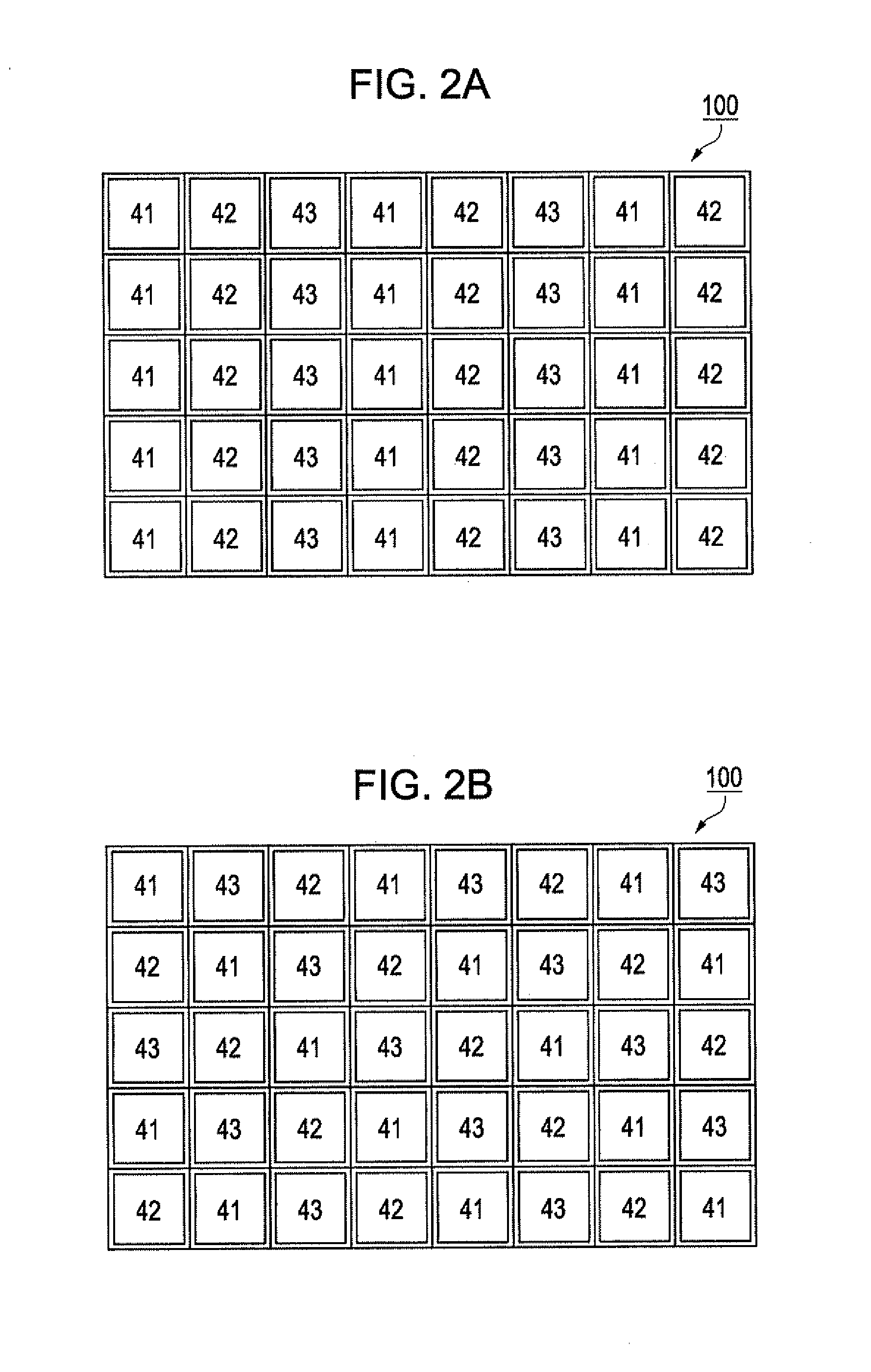
[0080]Next, the second embodiment of this invention will be described. The organic EL device 92 relating to the present embodiment has the same purpose of use and configuration as the organic EL device 91 relating to the first embodiment, and the components are also the same. That is, as shown in FIG. 1, both the first surface 3 and the second surface 4 have display regions 100 which substantially overlap in a plan view, and both of the surfaces (3, 4) can display images which are each different. In addition, due to the transmissive region 43 (refer to FIGS. 2A and 2B and the like) formed in the display region 100, the opposing side (that is, the opposite side) through the organic EL device can be visually recognized. The arrangement configuration of the three types of regions including the transmissive region 43 is also the same. That is, a column arrangement as shown in FIG. 2A has been adopted.
[0081]The organic EL device 92 is different from the organic EL device 91 of the first ...
third embodiment
[0109]Next, the third embodiment of this invention is described. An organic EL device 93 of the third embodiment is a double-sided display organic EL device in the same manner as the organic EL device in the embodiments described above. The provision of the transmissive region 43 is also the same. The difference is that color images are displayed on one surface (one side) and black and white images are display on the other surface (other side). Accordingly, the purpose of use and configuration are the same as both the organic EL device 91 and the organic EL device 92, and the components are also similar. Therefore, in the description below, configuration components which are common with configuration components of the organic EL devices (91, 92) described above are given the same symbols and a part of the description is not repeated.
[0110]FIG. 3C is a diagram illustrating an arrangement configuration of pixel regions in the display region 100 of the organic EL device 93. As shown in...
PUM
 Abstract
Description
Claims
Application Information