

Light emitting diode based linear lamps
- Summary
- Abstract
- Description
- Claims
- Application Information
AI Technical Summary
Benefits of technology
Problems solved by technology
Method used
Image

Examples
first embodiment
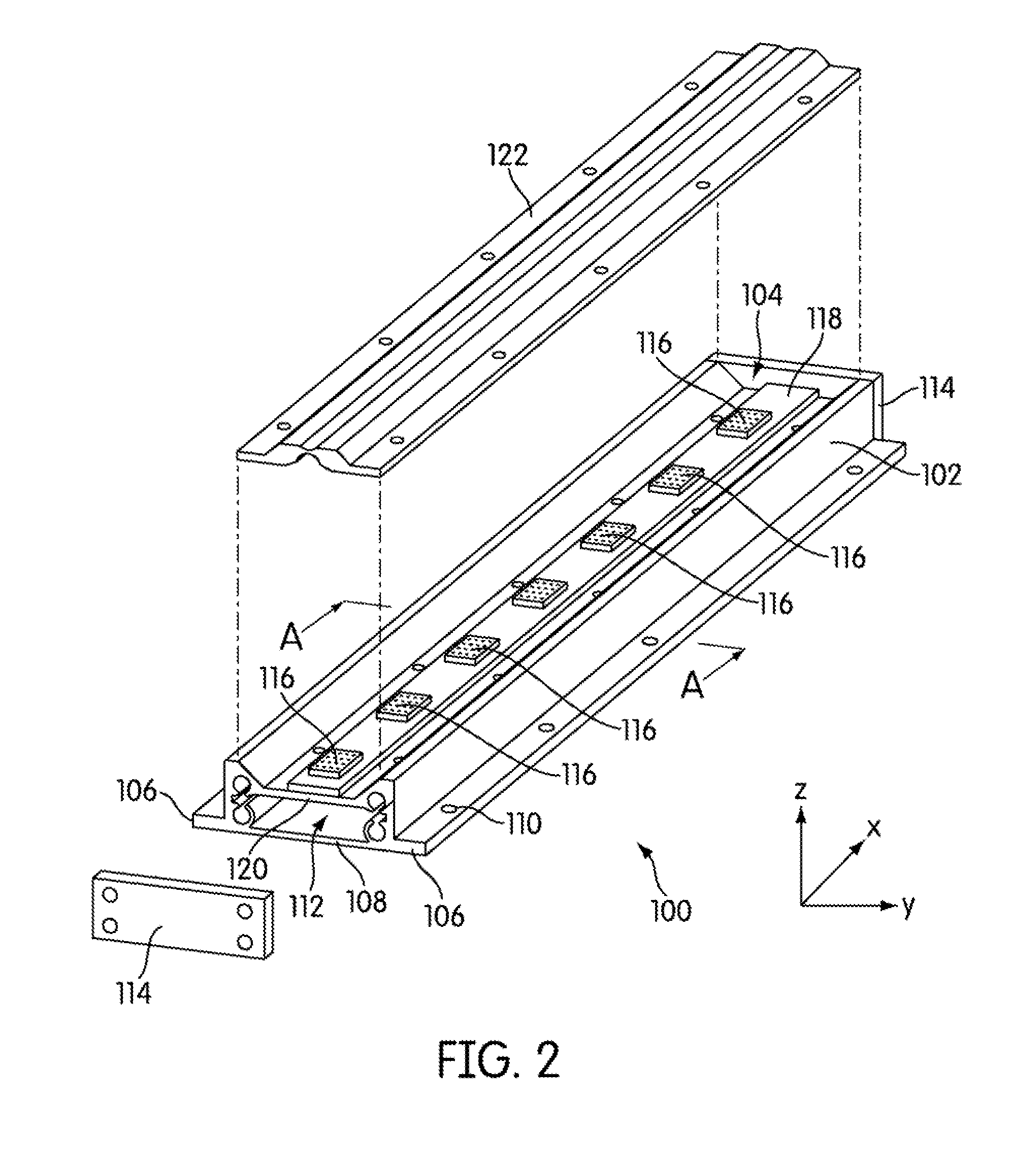
[0039]A linear lamp (lighting bar) 100 in accordance with the invention is now described with reference to FIGS. 2 and 3 which respectively show a partially exploded schematic perspective representation of the LED lighting bar and a sectional view of the LED lighting bar through a plane A-A. The lighting bar 100 is configured to generate white light with a Correlated Color Temperature (CCT) of ≈2700K, 3000K, 4000K or 6500K and an emission luminous flux of ≈560 lm (2700K, 3000K) or ≈600 lm (4000K, 6500K). The lighting bar 100 is intended, but not limited, to use within a light box (backlight) of a light emitting sign.
[0040]The lighting bar 100 comprises an elongate body 102 which for ease of fabrication comprises an extruded aluminum section. As shown in FIG. 2 the body 102 is hollow in form and has a generally rectangular cross-section with a shallow channel 104 in the upper surface and shoulders 106 projecting from the edges of the base 108. The walls of the channel 104 are beveled...
second embodiment
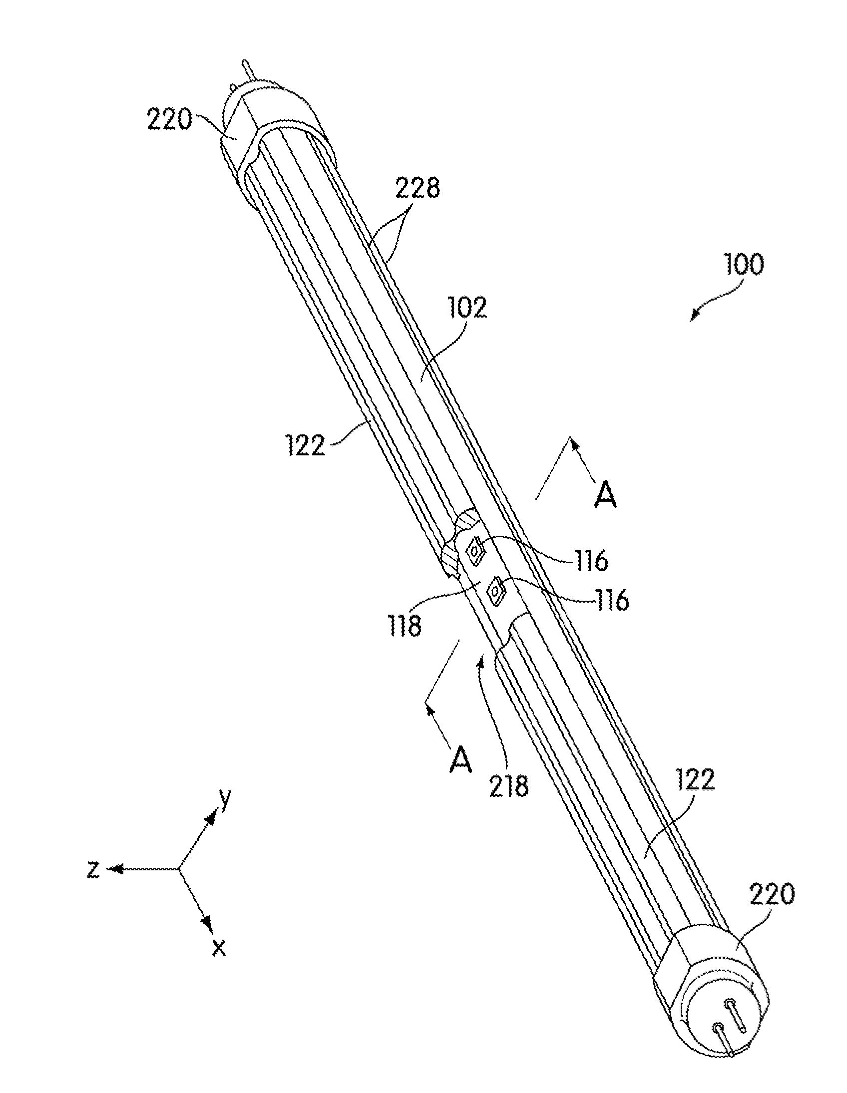
[0053]An LED linear lamp (tubular lamp) 100 in accordance with the invention is now described with reference to FIGS. 11 and 12 which respectively show a schematic perspective representation and a sectional view of the tubular lamp through a plane A-A. The tubular lamp 100 is configured to be a direct replacement for a “T8” fluorescent tube lamp. As is known fluorescent tubes are classified by the nomenclature “Tn” where “T” indicates the lamp is tubular in form and “n” is the diameter of the lamp in eights of an inch (⅛″). Thus the body of a T8 tubular lamp is nominally one inch (1″) in diameter. T8 fluorescent tubes are commonly used in backlit light emitting signage and the tubular lamp of the invention is intended for such applications.
[0054]In FIG. 11 a portion 218 of the lens 122 is removed to show the linear array of LEDs 116. The lamp 100 further comprises a bi-pin connector cap 220 attached to each end of the lamp body 102. It will be appreciated that depending on the inten...
PUM
 Abstract
Description
Claims
Application Information