Eureka AIR delivers breakthrough ideas for toughest innovation challenges, trusted by R&D personnel around the world.

Pitch division patterning techniques

a patterning and pitch division technology, applied in the field of semiconductor processing, can solve the problems of lithographic techniques that cannot reliably form features below a minimum pitch, the minimum pitch of lithographic techniques is an obstacle to feature size reduction, and the physical strength of the feature may not be enough to withstand processing environments

Active Publication Date: 2011-06-23
INTEL CORP
View PDF15 Cites 31 Cited by
  • Summary
  • Abstract
  • Description
  • Claims
  • Application Information

AI Technical Summary

Problems solved by technology

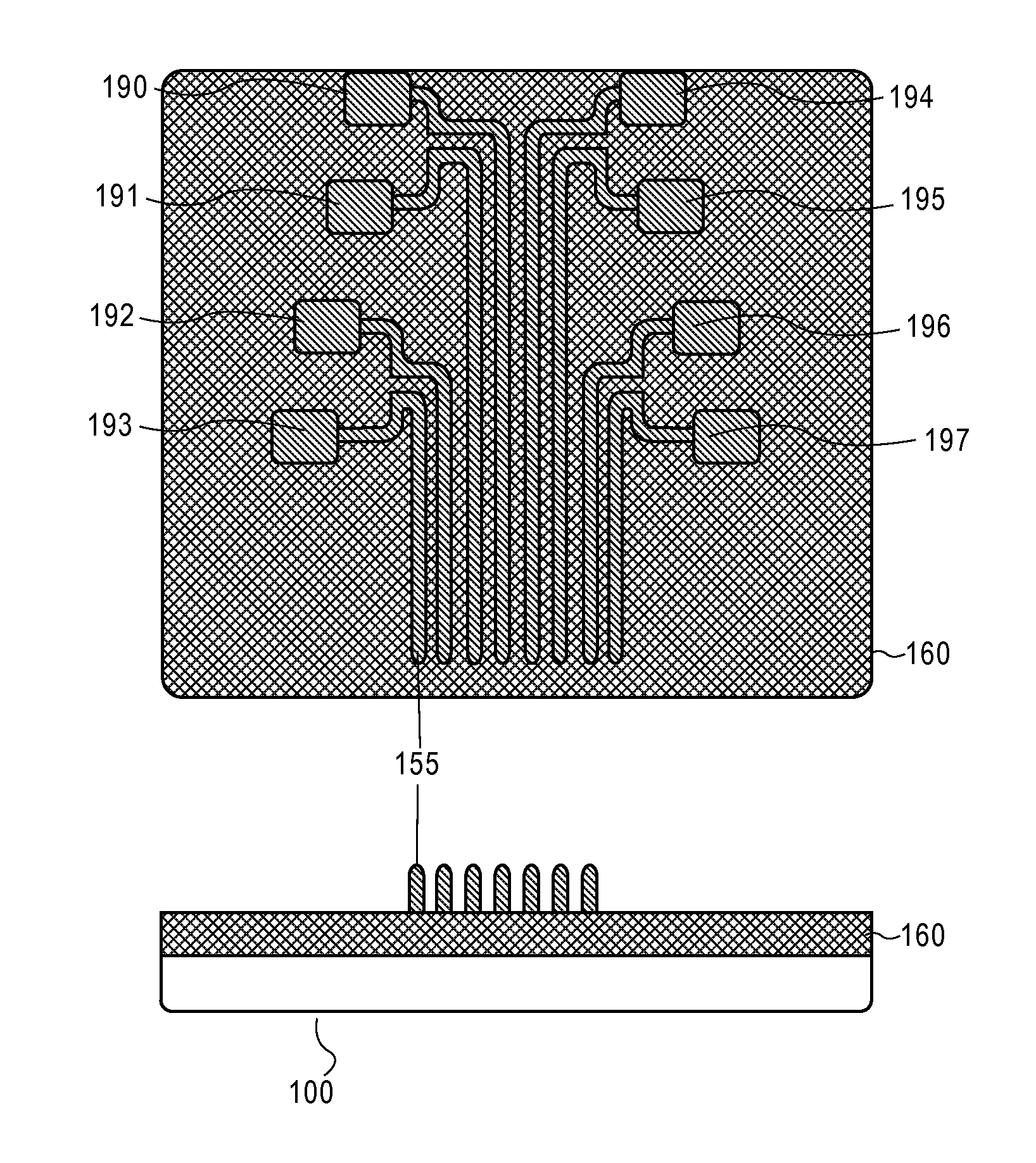
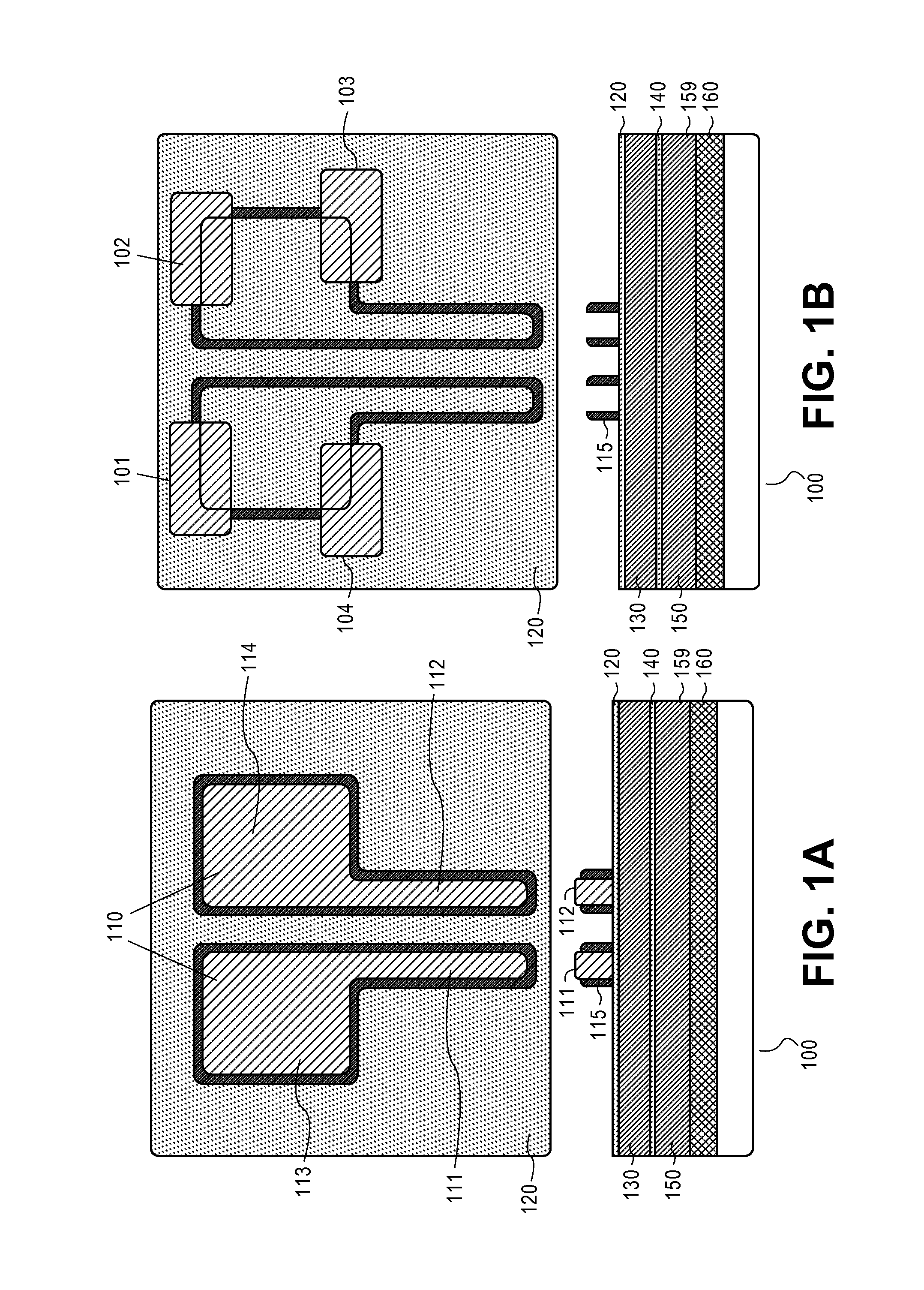
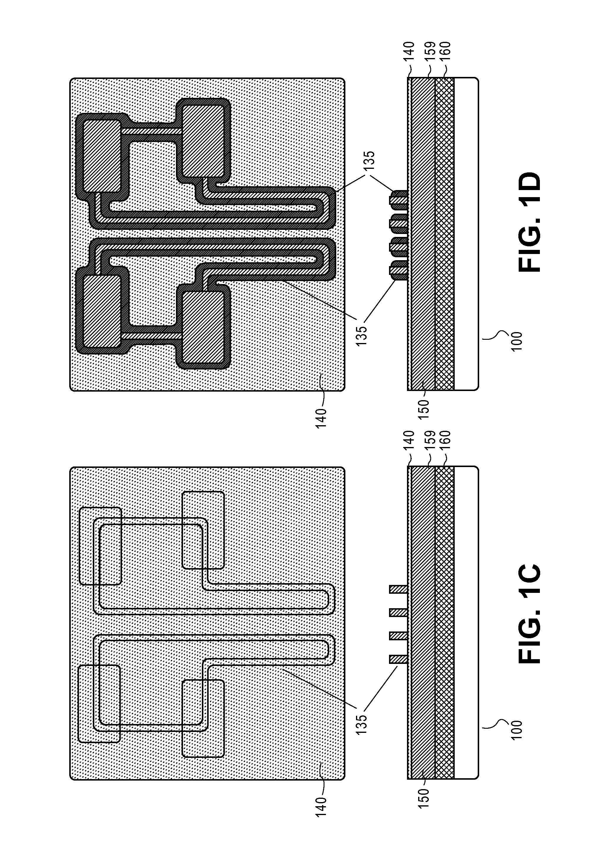
Lithographic techniques cannot reliably form features below a minimum pitch due to factors such as optics and light or radiation wavelength.
Thus, the minimum pitch of a lithographic technique is an obstacle to feature size reduction.
Furthermore, if feature size is shrunk below 15 nm, the physical strength of the feature may not be enough to withstand processing environments.
Pitch quad lines produced by prior art methods are susceptible to feature collapse due to capillary forces (e.g., moisture in the air, fluid processing) and shorting problems (because of the reduced space between the lines).

Method used


Image

  • Pitch division patterning techniques
  • Pitch division patterning techniques
  • Pitch division patterning techniques

Examples


Embodiment Construction

[0011]The following description provides examples, such as material types, etch chemistries, and processing conditions, in order to provide a thorough description of embodiments of the present invention; however, a person of ordinary skill in the art will understand the present invention may be practiced without employing these specific details.

[0012]Process acts and structures necessary to understand the embodiments of the present invention are described in detail below. The description below does not form a complete process flow for manufacturing a semiconductor device, and the semiconductor structures described below do not form a complete semiconductor device. Additional acts to form complete semiconductor devices from the semiconductor structures may be performed by fabrication techniques known in the art.

[0013]As described above, pitch quad techniques extend the capabilities of lithographic techniques beyond their minimum pitch. The pitch quad techniques described herein diffe...


PUM


Abstract

Embodiments of the invention comprise pitch division techniques to extend the capabilities of lithographic techniques beyond their minimum pitch. The pitch division techniques described herein employ additional processing to ensure pitch divided lines have the spatial isolation necessary to prevent shorting problems. The pitch division techniques described herein further employ processing acts to increase the structural robustness of high aspect ratio features.

Description

FIELD[0001]Embodiments of the invention generally pertain to semiconductor processing and more specifically to pitch division techniques and processing acts to increase physical stability of pitch divided lines.BACKGROUND[0002]Feature sizes for integrated circuits are continuously being reduced in response to many factors, including demand for increased portability, computing power, memory capacity and energy efficiency. Reduced feature sizes for integrated circuits are related to the techniques used to form said features. For example, lithography is commonly used to pattern features (e.g., conductive lines) of integrated circuits. The periodicity of these patterned features maybe described as a pitch.[0003]Pitch describes the distance between identical points of two neighboring features. Lithographic techniques cannot reliably form features below a minimum pitch due to factors such as optics and light or radiation wavelength. Thus, the minimum pitch of a lithographic technique is a...

Claims


Application Information

Patent Timeline
IPC IPC(8): H01L21/033
CPCH01L21/0337H01L21/0338H01L21/3086H01L21/76816H01L21/31144H01L21/32139H01L21/76224H01L21/3088H01L21/76885H01L23/528G03F1/80H01L21/0274
Inventor TANG, SANH D.SILLS, SCOTTLIU, HAITAO
Owner INTEL CORP
Why Eureka
Eureka Blog
Learn More