Electric optical apparatus, driving method thereof and electronic device

a technology of optical apparatus and driving method, applied in the direction of electric digital data processing, instruments, computing, etc., can solve problems such as uneven display, and achieve the effect of reducing uneven display and high quality

Active Publication Date: 2011-07-14
E INK CORPORATION
View PDF26 Cites 32 Cited by
  • Summary
  • Abstract
  • Description
  • Claims
  • Application Information

AI Technical Summary

Benefits of technology

[0049]According to the invention, the electronic device can be obtained with high quality image display, which decreases the unevenness display.

Problems solved by technology

Thus, the current Is is varied in each of the pixels and display tones are different to each other so that unevenness display occurs.

Method used


Image

  • Electric optical apparatus, driving method thereof and electronic device
  • Electric optical apparatus, driving method thereof and electronic device
  • Electric optical apparatus, driving method thereof and electronic device

Examples


first embodiment

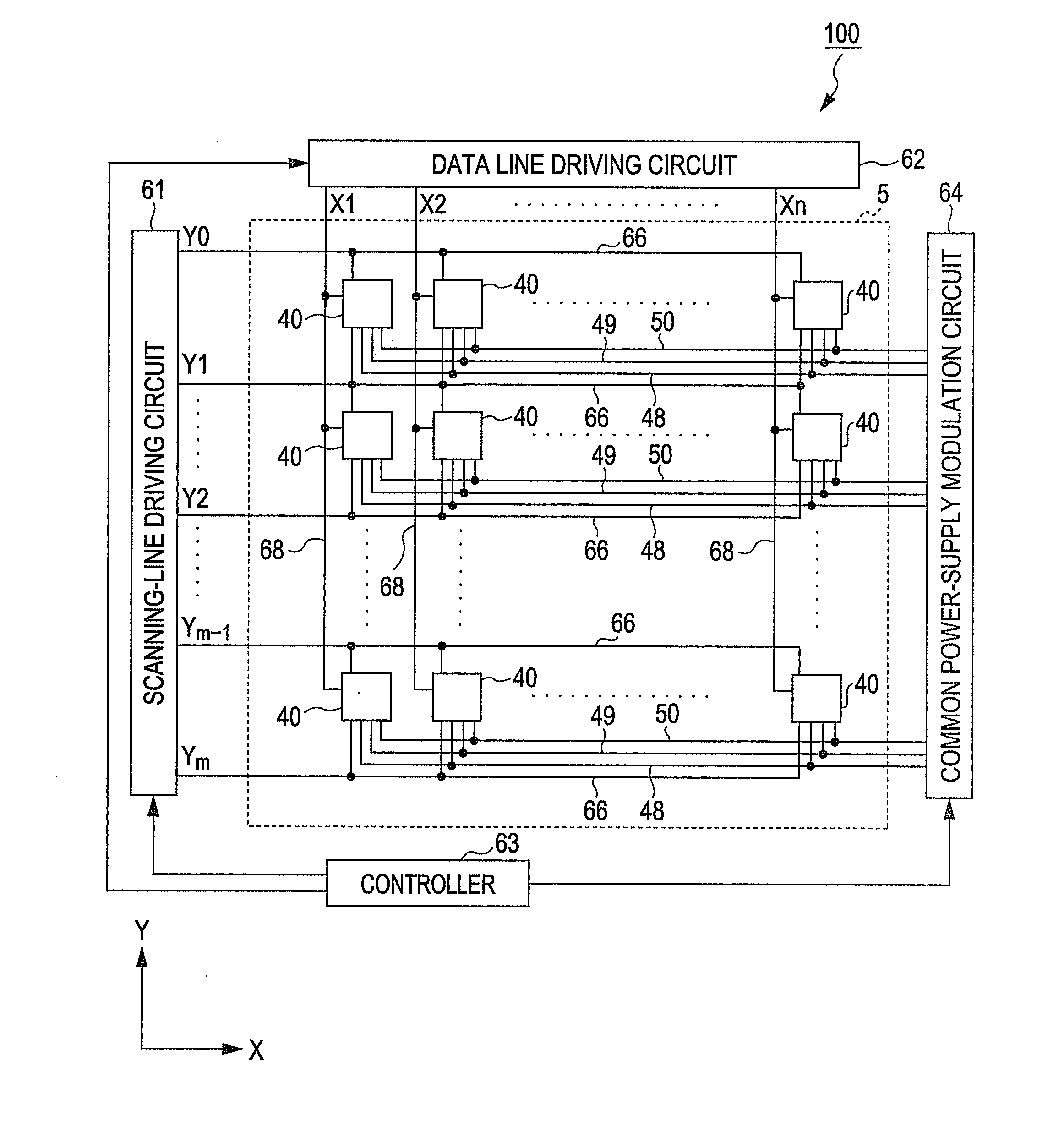
[0069]FIG. 1 is a schematic configuration view showing an electrophoretic display apparatus 100 according to a first embodiment of an electric optical apparatus of the invention.

[0070]The electrophoretic display apparatus 100 includes a display section 5 in which a plurality of pixels 40 is arranged in a matrix shape. A scanning line driving circuit 61, a data line driving circuit 62, a controller (control section) 63 and a common power-supply modulation circuit 64 are arranged in the vicinity of the display section 5. The scanning line driving circuit 61, the data line driving circuit 62, and the common power-supply modulation circuit 64 are each connected to the controller 63. The controller 63 entirely controls those on the basis of image data or synchronizing signals that are supplied from an upper rank apparatus.

[0071]A plurality of scanning lines 66 that is extended from the scanning line driving circuit 61 and a plurality of the data lines 68 that is extended from the data li...

modified example

[0121]FIG. 7 is a timing chart showing a modified example of a driving method according the first embodiment.

[0122]In the modified example of FIG. 7, a ramp waveform is input to the source (power-supply line 50) of the driving transistor TRd in the display driving step S104 in which the electrophoretic element 32 is driven and the image is displayed. In other words, the common power-supply modulation circuit 64 illustrated in FIG. 1 is configured such that a predetermined shaped ramp waveform can be freely input with respect to the plurality of power-supply lines 50. Also, the image signals input step S10 is the same as that of the first embodiment.

[0123]In the driving method of the example, the ramp waveform that is supplied to the power-supply lines 50 is gradually changed to the negative voltage and the voltage Vgs between gate-source of the driving transistor TRd is gradually increased from the start of the input of the ramp waveform as shown in FIG. 7. As illustrated in below E...

second embodiment

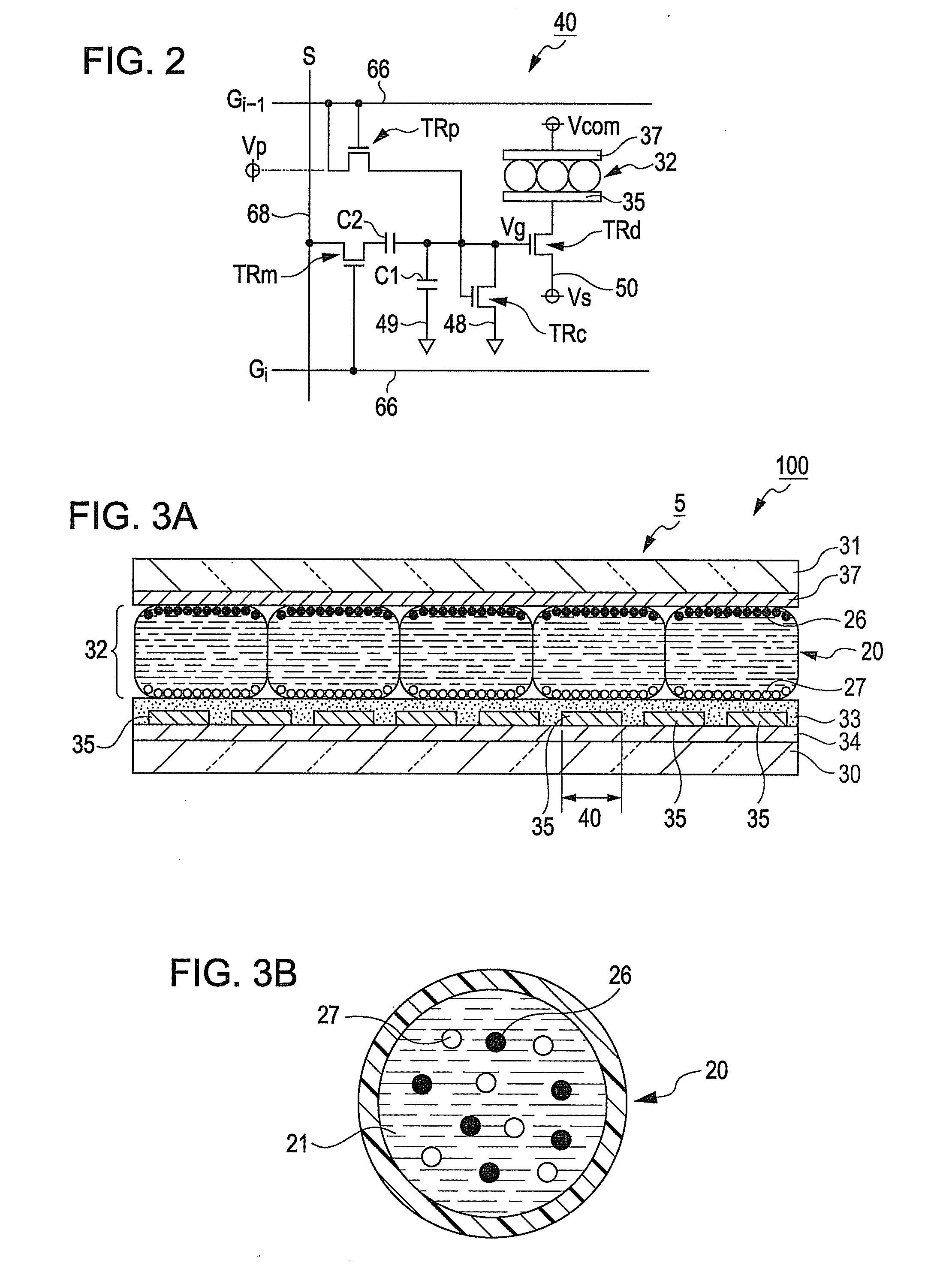
[0126]FIG. 8 is a view showing a pixel circuit of the electrophoretic display apparatus according to a second embodiment. The electrophoretic display apparatus of the embodiment includes a configuration of a pixel 240 illustrated in FIG. 8 instead of the pixel 40 according to the first embodiment.

[0127]The electrophoretic display apparatus of the embodiment has a basic configuration similar to the electrophoretic display apparatus 100 according to the above-described first embodiment and the constituent elements similar to the first embodiment are given the same reference numbers thereof, and are thus are not specifically described in the below description and reference drawings.

[0128]The driving transistor TRd, the transistor for correction TRc, the transistor for precharge TRp, the maintenance capacitance C1, the capacitance for modulation C2, the pixel electrode 35, the electrophoretic element 32 and the common electrode 37 are provided in the pixel 240 shown in FIG. 8. Also, the...


PUM

PropertyMeasurementUnit
particle diameteraaaaaaaaaa
capacitanceaaaaaaaaaa
maintenance capacitanceaaaaaaaaaa

Abstract

An electric optical apparatus including a display section in which an electric optical material is pinched between a pair of substrates and a plurality of pixels is arranged, wherein the display section is provided with a scanning line, a data line and a power-supply line that are connected to each of the pixels, and each of the pixels is provided with a pixel electrode, a driving transistor that is connected between the pixel electrode and the power-supply line, a capacitance for modulation that is connected between a gate of the driving transistor and the data line, a maintenance capacitance that connects one side electrode to the gate of the driving transistor, and a transistor for correction that is connected to a diode and in which one side terminal thereof is connected to the gate of the driving transistor.

Description

CROSS-REFERENCE TO RELATED APPLICATION[0001]This application is based on and claims priority from Japanese Patent Application No. 2010-004173, filed on Jan. 12, 2010, the contents of which are incorporated herein by reference.BACKGROUND[0002]1. Technical Field[0003]The present invention relates to an electric optical apparatus, a driving method thereof and an electronic device.[0004]2. Related Art[0005]An electrophoretic display apparatus that includes a control transistor, a maintenance capacitance and a driving transistor within a pixel is known in the related art (for example, JP-A-2008-176330). In the pixel of the electrophoretic display apparatus described in JPA-2008-176330, the maintenance capacitance is charged by an image signal that is input through the control transistor and the driving transistor flows a current to a pixel electrode according to a voltage of the maintenance capacitance. Thus, brightness display can be obtained according to an amount of charge (current×ti...

Claims


Application Information

Patent Timeline
Patent Type & Authority Applications(United States)
IPC IPC(8): G09G5/00
CPCG09G3/344G09G2300/0852G09G3/3446G09G2310/06G09G2310/0251G09G2300/0819G09G3/3233G09G5/00
Inventor YAMAZAKI, KATSUNORI
Owner E INK CORPORATION
Why Eureka
Try Eureka