Compact image sensor arrangement

a compact, image sensor technology, applied in the field of image sensors, can solve the problem of increasing the overall size of the image sensor

Active Publication Date: 2011-07-28
STMICROELECTRONICS SRL +1
View PDF12 Cites 60 Cited by
  • Summary
  • Abstract
  • Description
  • Claims
  • Application Information

AI Technical Summary

Benefits of technology

Embodiments of the present disclosure aim to at least partially address one or more problems in the prior art.

Problems solved by technology

However, there is a problem in doing so without increasing the overall size of the image sensor.

Method used


Image

  • Compact image sensor arrangement
  • Compact image sensor arrangement
  • Compact image sensor arrangement

Examples


Embodiment Construction

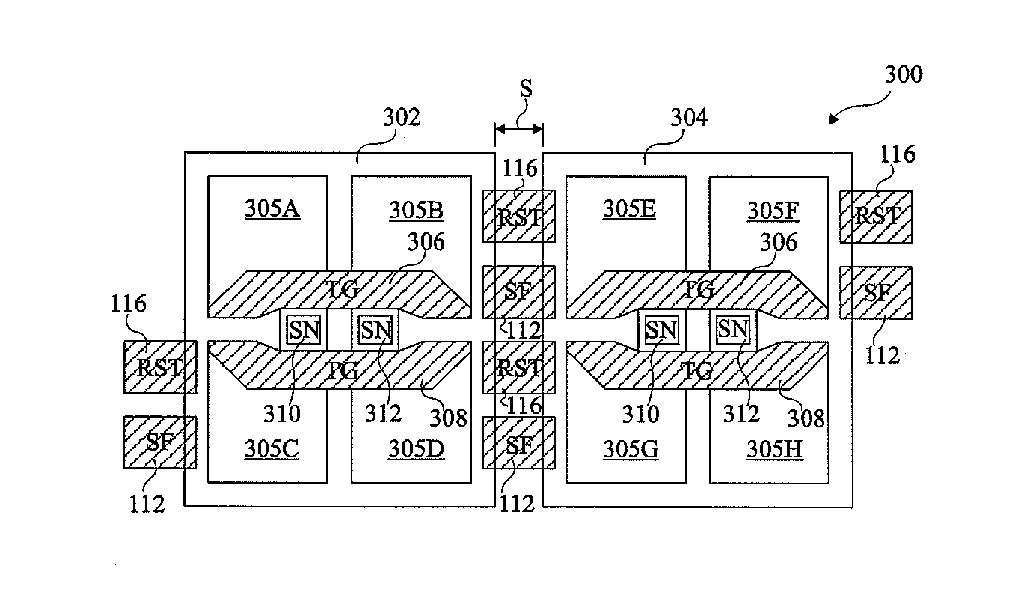
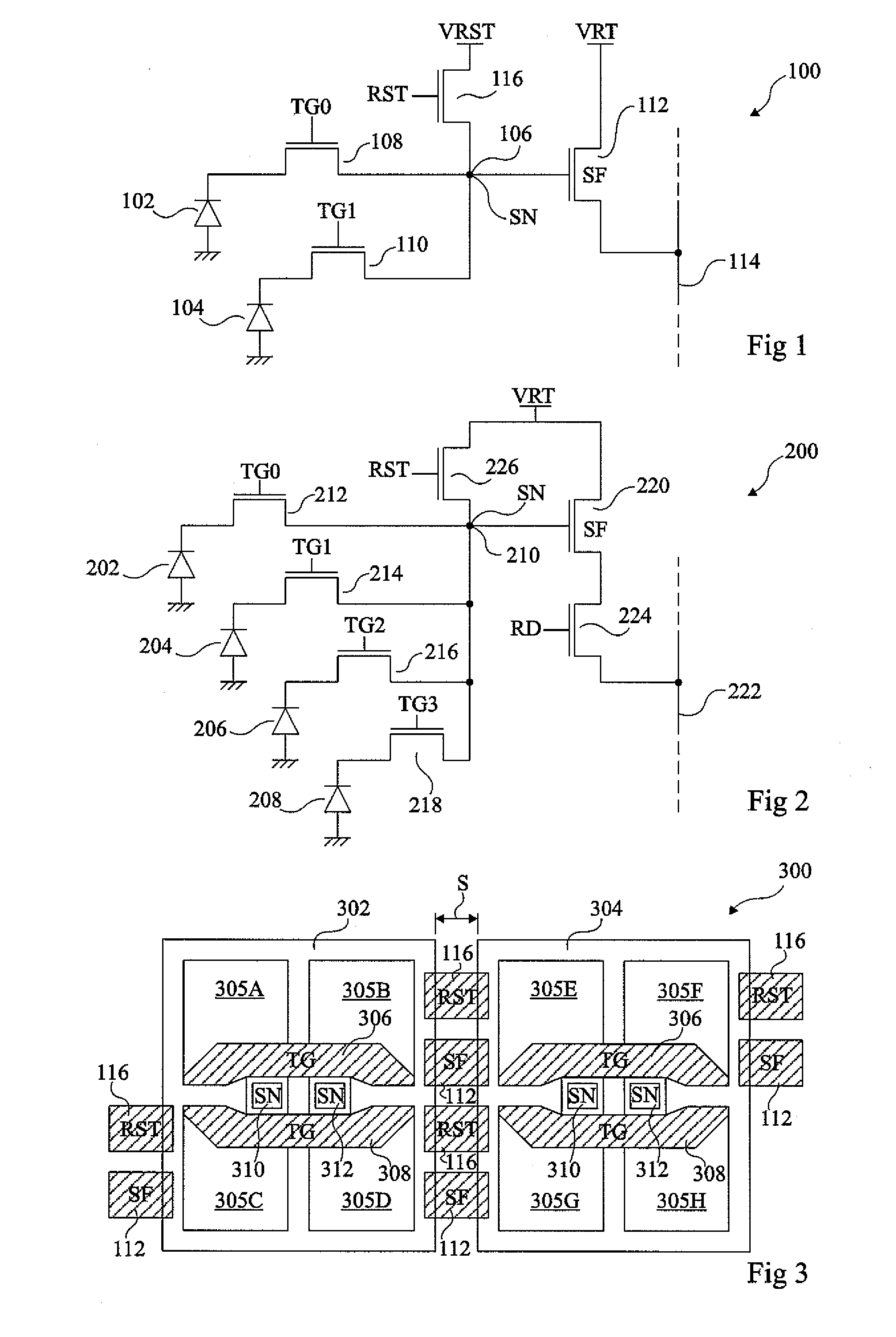
FIGS. 1 and 2 illustrate examples of 2T and 1T75 pixel circuits respectively.

Pixel circuit 100 of FIG. 1 comprises two pinned photodiodes 102 and 104, each coupled to a sensing node (SN) 106 via a respective transfer transistor 108, 110. Transistors 108 and 110 are for example MOS transistors receiving, at their respective gates, transfer voltages TG0 and TG1. The sensing node 106 is further coupled read circuitry. In particular the sensing node is coupled to the gate of a source follower transistor 112, which has its drain coupled to a supply voltage VRT, and its source to coupled to a column line 114, and to a reset voltage VRST via a reset transistor 116, which receives a reset signal RST at its gate.

The pixel circuitry 200 of FIG. 2 comprises four pinned photodiodes 202, 204, 206 and 208, each of which is coupled to a sensing node (SN) 210 via a respective transfer transistor 212, 214, 216 and 218. The transfer transistors 212 to 218 are, for example, MOS transistors, and receiv...


PUM


Abstract

An image sensor having a number of pixel zones delimited by isolation trenches, each pixel zone including a photodiode; a transfer gate associated with each of the pixel zones and arranged to transfer charge from the photodiode to a sensing node; and a read circuit for reading a voltage at one of the sensing nodes, the read circuitry including a number of transistors of which at least one is positioned at least partially over a pixel zone of the pixel zones.

Description

CROSS REFERENCE TO RELATED APPLICATIONSThis application claims the priority benefit of French patent application number 10 / 50572, filed on Jan. 28, 2010 entitled“Compact Image Sensor Arrangement,” which is hereby incorporated by reference to the maximum extent allowable by law.BACKGROUND OF THE INVENTION1. Field of the InventionThe present invention relates to an image sensor and a method of forming an image sensor, and in particular to an image sensor comprising an array of pixels.2. Discussion of the Related ArtMonolithic image sensors comprise photodiodes and transistors formed in a silicon substrate. More specifically, such image sensors comprise in array of pixels each having a pinned photodiode coupled to a sensing node by a transfer transistor. A charge accumulated by the photodiode during an integration period can be transferred to the sensing node via the transfer transistor.Reading the voltage stored at the sensing node is performed using read circuitry, generally comprisi...

Claims


Application Information

Patent Timeline
Patent Type & Authority Applications(United States)
IPC IPC(8): H01L27/146H01L31/18
CPCH01L27/14603H01L27/14609H01L21/76816H01L27/14641H01L21/76229H01L21/762H01L27/1464H01L21/76232
Inventor ROY, FRANCOISBARBIER, FREDERIC
Owner STMICROELECTRONICS SRL
Why Eureka
Try Eureka