Deposition apparatus and method

Active Publication Date: 2011-08-25
TOYOTA JIDOSHA KK +3
View PDF11 Cites 19 Cited by
  • Summary
  • Abstract
  • Description
  • Claims
  • Application Information

AI Technical Summary

Benefits of technology

[0026]In another embodiment of this invention; a deposition method for depositing a film on a substrate placed on a susceptor installed within a chamber by supplying deposition gas from a top section of the chamber toward the substrate while heating the substrate with the use of an electric resistance heater located below the substrate, wherein an upper electric resistance heater cluster is located between inner walls of the chamber and a liner, provided inside the chamber, for covering the inner walls of the chamber, such that the upper electric resistance heater cluster surrounds the liner, wherein the upper electric resistance heater cluster is divided vertically into a plurality of electric resistance heaters so that the plurality of electric resistance heaters can be independently temperature-controlled and wherein the film is deposited by heating the substrate while performing temperature control on both the electric resistance heater located below the substrate and the upper electric resistance heater cluster.

Problems solved by technology

However, difficulties are involved in using an electric resistance heater to heat the substrate 206 up to such a high temperature as stated above because the connectors for electrically connecting the heater and electrodes are low in thermal resistance.
In other words, it is difficult to apply resistance heating for heating the substrate 206 up to more than 1,500 degrees Celsius.
However, the use of the high-frequency induction heater, which is located at a chamber side-wall section, creates the following problem: the heating effect of the high-frequency induction heater varies depending on its distance from a substrate to be heated.
This renders fine and precise temperature control of the induction heater almost impossible.
Therefore, the use of an electric resistance heater and a high-frequency induction heater results in less precise temperature control of heating means as a whole despite the precise temperature control capabilities of the electric resistance heater.

Method used


Image

  • Deposition apparatus and method
  • Deposition apparatus and method
  • Deposition apparatus and method

Examples


Embodiment Construction

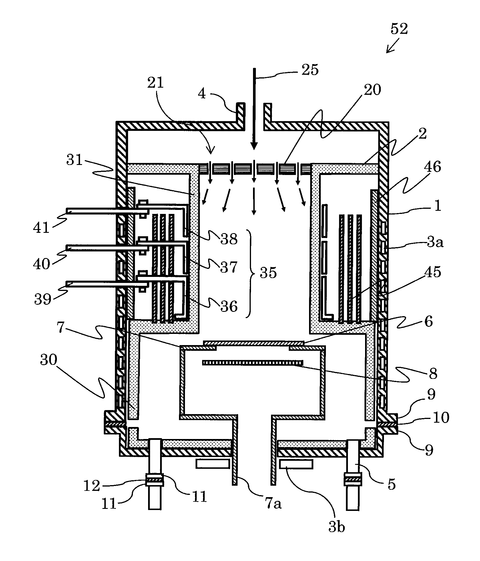
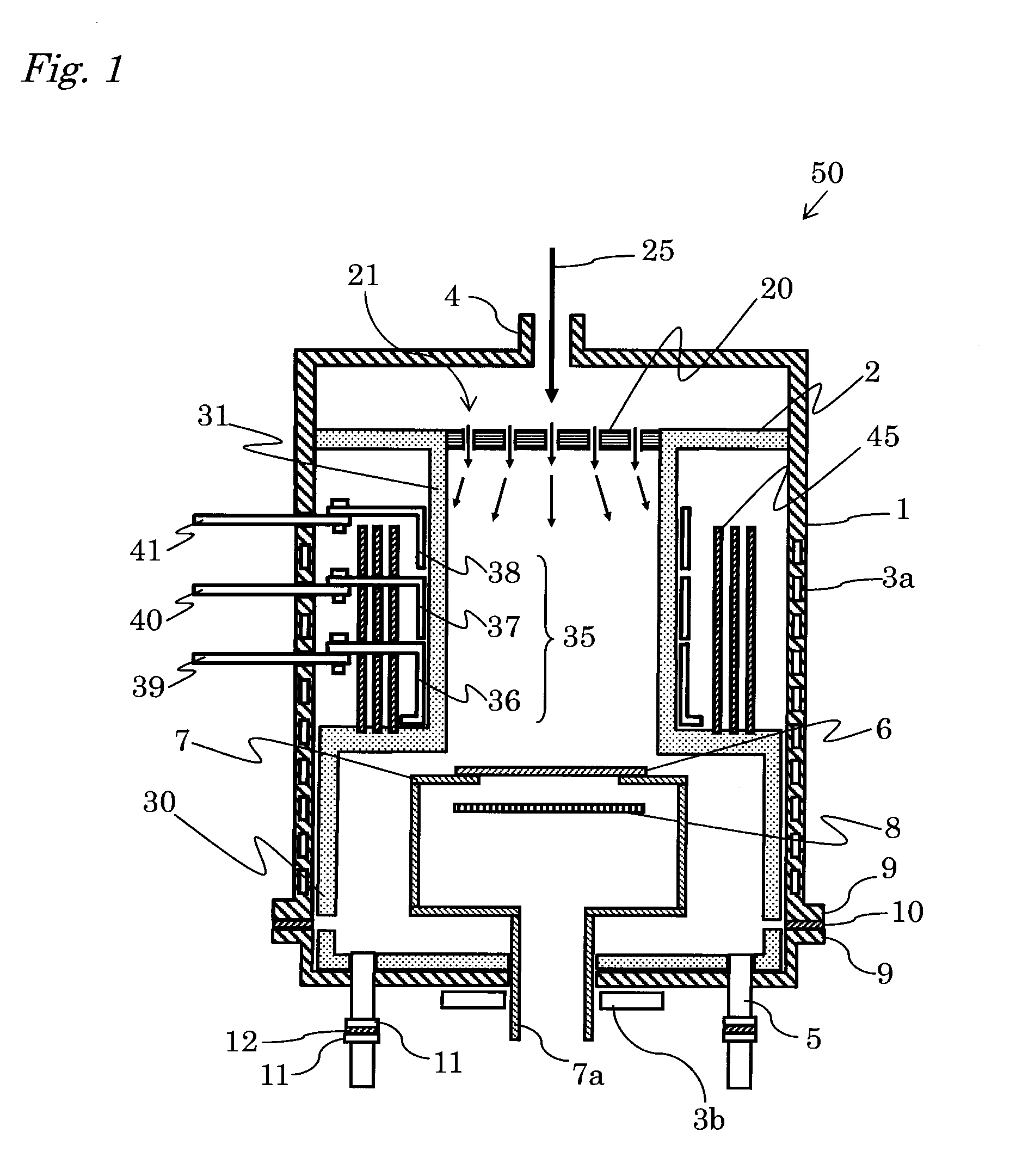
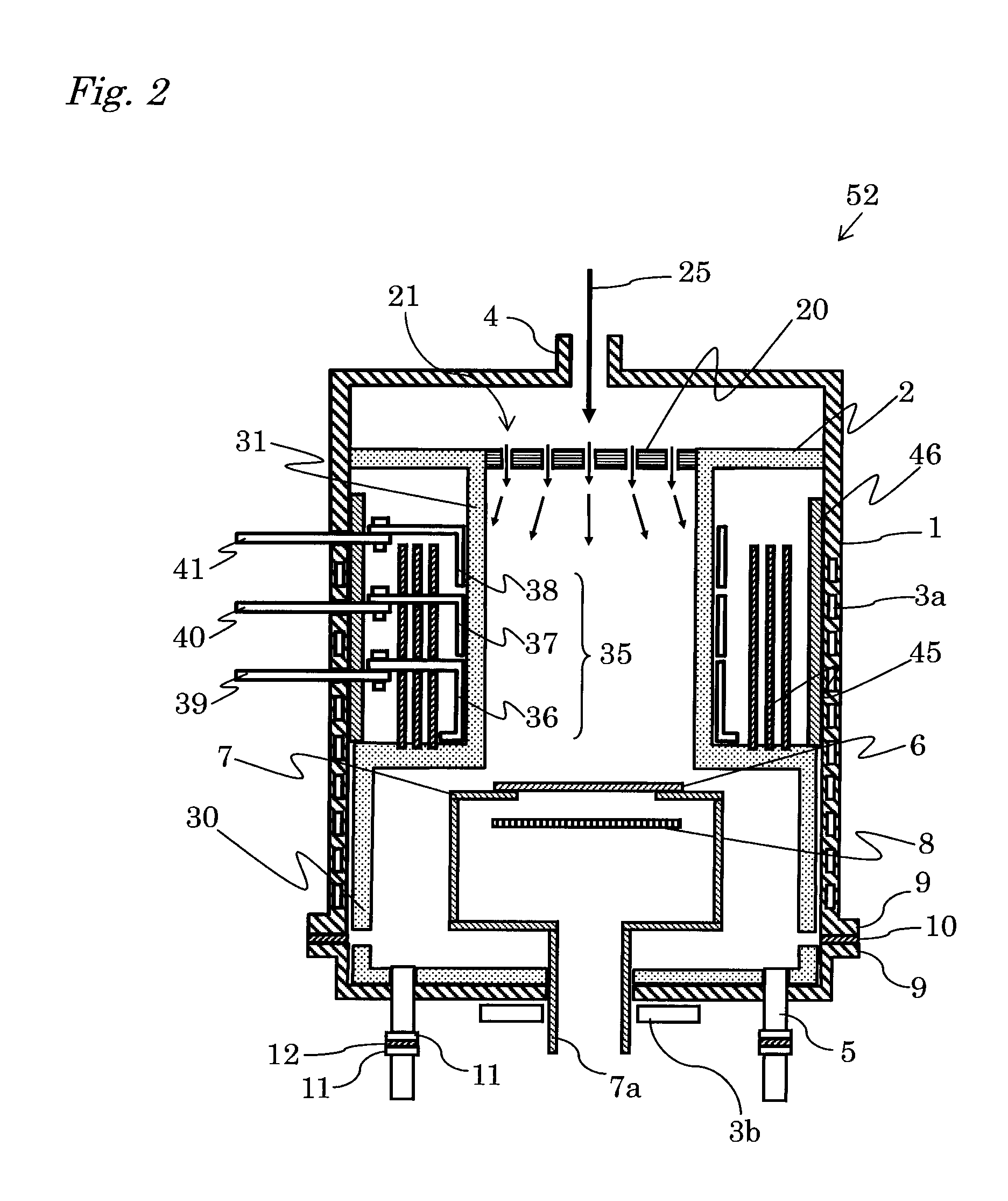
[0030]FIG. 1 is a schematic cross section of a film deposition apparatus 50 according to an embodiment of the invention. In this preferred embodiment, the deposition apparatus 50 is designed to deposit an SiC (silicon carbide) crystalline film on the top surface of a substrate 6. The substrate 6 is thus a SiC wafer. Of course, it is also possible to use other wafers formed of different materials if so required. Examples of alternative wafers include an Si wafer, other insulative wafers such as an SiO2 (quartz) wafer and the like, and semi-insulative wafers such as a high-resistance gallium arsenide (GaAs) wafer and the like.

[0031]The deposition apparatus 50 of FIG. 1 comprises the following components: a film deposition chamber 1 having upper and lower sections; a hollow liner 2 located inside the chamber 1 to protect its inner walls; coolant passageways 3a and 3b through which coolant water flows to cool the chamber 1; a gas inlet 4 from which to introduce a deposition gas 25; gas ...


PUM

PropertyMeasurementUnit
Temperatureaaaaaaaaaa
Electrical resistanceaaaaaaaaaa

Abstract

A deposition apparatus 50 includes a chamber 1 having at its top section a gas inlet 4 for supplying deposition gas 25. Inside chamber 1 is a susceptor 7 on which to place a substrate 6; a heater 8 located below the substrate 6; and a liner 2 for covering the inner walls of the chamber 1. Apparatus 50 deposits a film on the substrate 6 by supplying deposition gas 25 from gas inlet 4 into chamber 1 while heating substrate 6. An upper electric resistance heater cluster 35 is located between the inner walls of the chamber 1 and liner 2 such that the upper heater 35 surrounds the liner 2. The upper heater 35 is divided vertically into electric resistance heaters 36, 37, and 38 which are independently temperature-controlled. The substrate 6 is heated with the use of both heater 8 and the upper heater cluster 35.

Description

BACKGROUND OF THE INVENTION[0001]1. Field of the Invention[0002]The present invention relates to a film deposition apparatus and a film deposition method.[0003]2. Background Art[0004]Epitaxy or epitaxial growth is often employed in manufacturing semiconductor devices that require relatively thick crystalline films. Examples of these devices include power semiconductor devices such as insulated-gate bipolar transistors (IGBTs) and the like.[0005]Vapor-phase epitaxy, a form of epitaxial growth, requires that the film deposition chamber in which a semiconductor substrate (e.g., a silicon wafer) has been placed be kept at atmospheric pressure (0.1 MPa or 760 Torr) or lower. After the substrate has been heated up to a given temperature, the chamber is supplied with a deposition gas which includes a reactive gas. When the deposition gas reaches the surface of the heated substrate, the reactive gas undergoes thermal decomposition or hydrogen reduction, thereby depositing an epitaxial film ...

Claims


Application Information

Patent Timeline
IPC IPC(8): C23C14/26C23C16/48
CPCC23C16/4557
Inventor SUZUKI, KUNIHIKOMITANI, SHINICHI
Owner TOYOTA JIDOSHA KK
Why Eureka
Try Eureka