Method of Forming a DRAM Array of Devices with Vertically Integrated Recessed Access Device and Digitline

a technology of recessed access devices and dram arrays, applied in the field of forming dram arrays, can solve the problems of limiting the scaling of such devices to smaller footprints and higher densities, and the component size of the device may become smaller and/or denser for a given storage capacity

Active Publication Date: 2011-09-15
MICRON TECH INC
View PDF4 Cites 52 Cited by
  • Summary
  • Abstract
  • Description
  • Claims
  • Application Information

AI Technical Summary

Problems solved by technology

As the footprints of such devices become smaller, the components of the device may become smaller and/or denser for a given storage capacity.
In such devices, construction of the

Method used


Image

  • Method of Forming a DRAM Array of Devices with Vertically Integrated Recessed Access Device and Digitline
  • Method of Forming a DRAM Array of Devices with Vertically Integrated Recessed Access Device and Digitline
  • Method of Forming a DRAM Array of Devices with Vertically Integrated Recessed Access Device and Digitline

Examples


Embodiment Construction

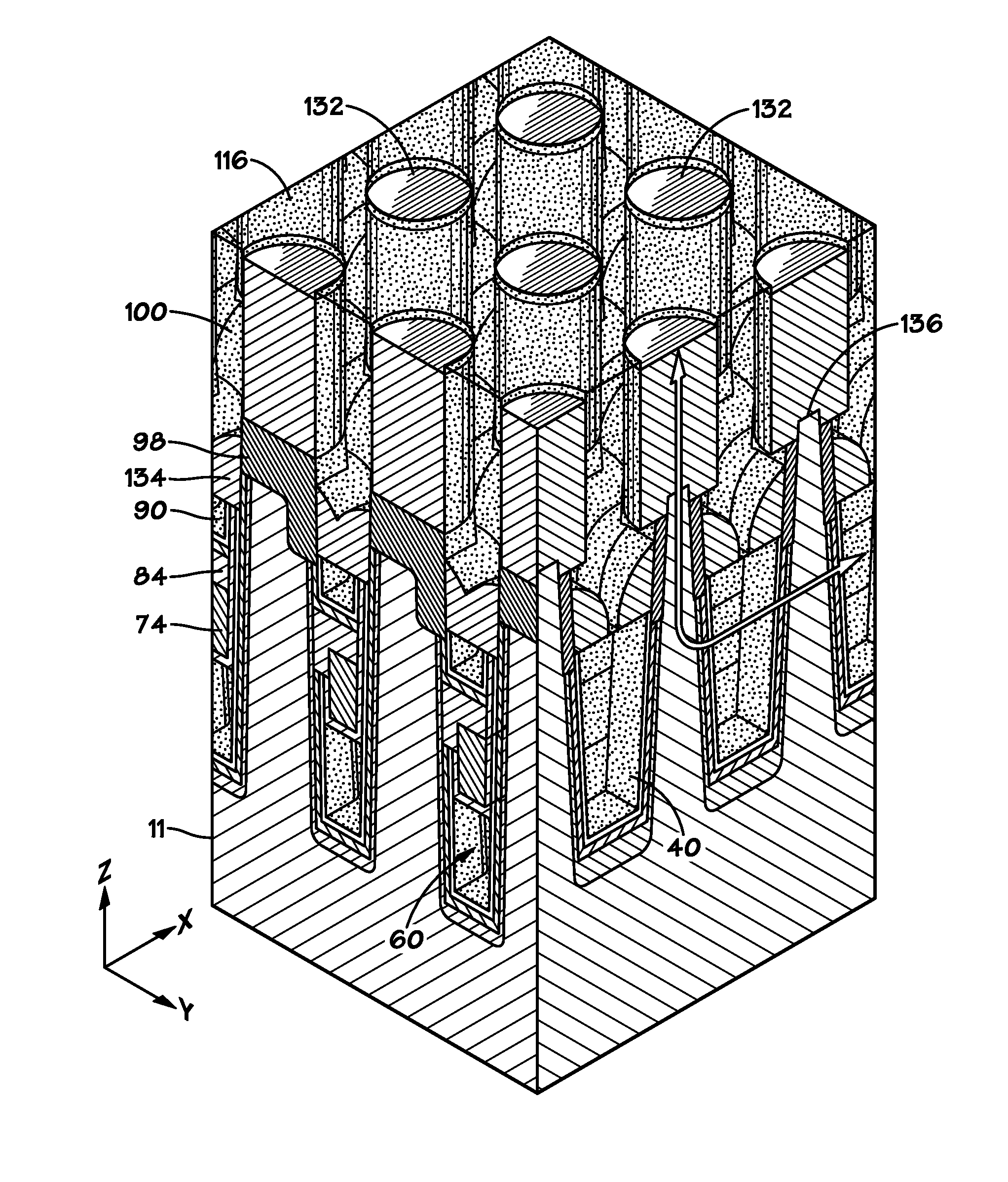
[0008]An embodiment of a process for fabricating a vertical cell configuration structure 10 (e.g., a DRAM device) having buried access lines, for example wordlines, and buried data / sense lines, for example digitlines, is described below with reference to FIGS. 1-24. The process may provide increased area for the construction of storage node contacts in 4F2 architectures and may maximize the area available for construction of such contacts (or other vertical structures) by constructing the digitlines below the contact area. Additionally, each subsurface (also referred to as “buried”) digitline may be electrically coupled to the silicon substrate via a single-sided digitline contact (also referred to as a single-sided strap). It should be appreciate that the techniques described below may also be implemented in embodiments having greater than 4F2.

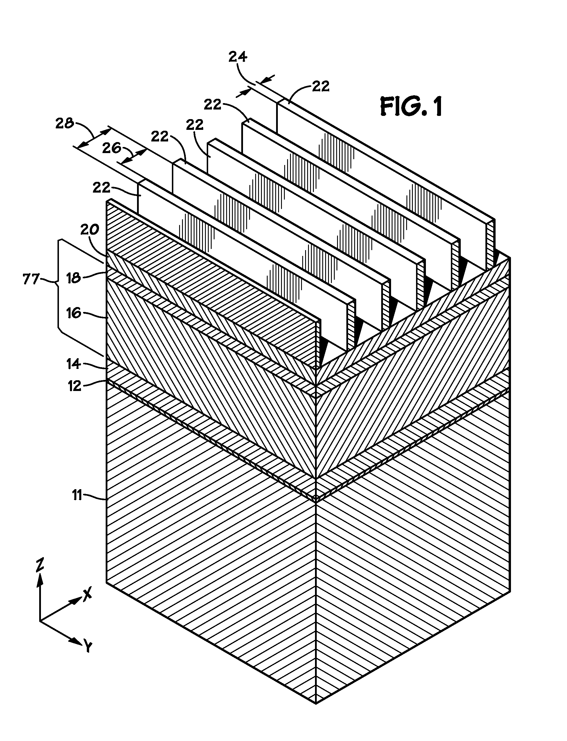
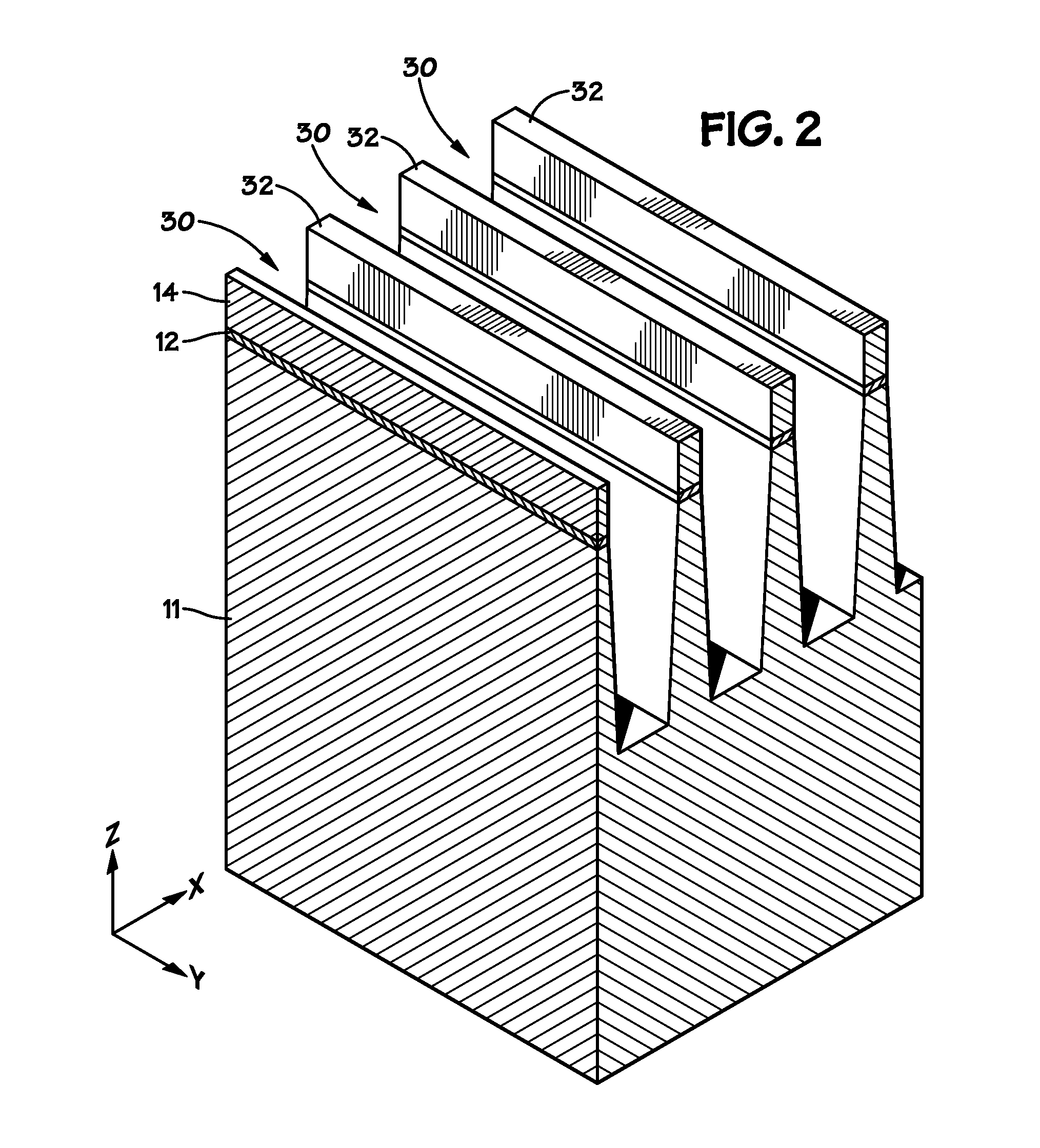
[0009]FIG. 1 illustrates a first step in an embodiment of a process for forming a vertical cell DRAM device. FIGS. 1-3 depict a shallow tren...


PUM


Abstract

A method is disclosed for forming a memory device having buried access lines (e.g., wordlines) and buried data/sense lines (e.g., digitlines) disposed below vertical cell contacts. The buried wordlines may be formed trenches in a substrate extending in a first direction, and the buried digitlines may be formed from trenches in a substrate extending in a second direction perpendicular to the first direction. The buried digitlines may be coupled to a silicon sidewall by a digitline contact disposed between the digitlines and the silicon substrate.

Description

BACKGROUND[0001]1. Field of Invention[0002]Embodiments of the invention relate generally to semiconductor devices and, more particularly, to methods of fabrication of such semiconductor devices having buried digitlines and wordlines.[0003]2. Description of Related Art[0004]Many types of electronic devices include data cells with a single transistor. Typically, the transistor controls whether a stimulus (e.g., a current or voltage) is applied to, or by, a data element (e.g., a memory element, an imaging element, or other device configured to output data, such as various kinds of sensors). Often a large number of data elements are disposed in an array, and the transistor allows individual data elements in the array to be selected. For example, certain types of dynamic random access memory (DRAM) cells include both a capacitor, which functions as a data element, and a single transistor, which functions as an access device, connected to the capacitor. The capacitor usually stores data b...

Claims


Application Information

Patent Timeline
IPC IPC(8): H01L29/78H01L21/28
CPCH01L27/10882H01L27/108H01L27/10891H01L27/10885H10B12/48H10B12/488H10B12/482H10B12/00
Inventor PAREKH, KUNALROBERTS, CEREDIGTRAN, THYJOZWIAK, JIMHWANG, DAVID
Owner MICRON TECH INC
Why Eureka
Try Eureka